TUSB1310A
www.ti.com
SLLSE32D–NOVEMBER 2010–REVISED MAY 2011
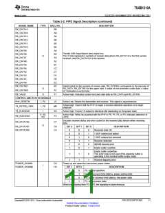
Table 2-2. PIPE Signal Description (continued)
SIGNAL NAME
TYPE
BALL NO.
B9
DESCRIPTION
RX_DATA15
RX_DATA14
RX_DATA13
RX_DATA12
RX_DATA11
RX_DATA10
RX_DATA9
RX_DATA8
RX_DATA7
RX_DATA6
RX_DATA5
RX_DATA4
RX_DATA3
RX_DATA2
RX_DATA1
RX_DATA0
RX_DATAK1
A9
A8
B8
B5
B4
A4
Parallel USB SuperSpeed data output bus.
The 16 bits represent 2 symbols of receive data where RX_DATA7-0 is the first symbol
received, and RX_DATA15-8 is the second.
B3
O
A3
A2
B1
C2
C1
D1
D2
E2
B7
Data/Control for the symbols of receive data. RX_DATAK0 corresponds to the low-byte of
RX_DATA, RX_DATAK1 to the upper byte. A value of zero indicates a data byte; a value
of 1 indicates a control byte.
O
O
RX_DATAK0
RX_VALID
A7
F1
Active High. Indicates symbol lock and valid data on RX_DATA and RX_DATAK.
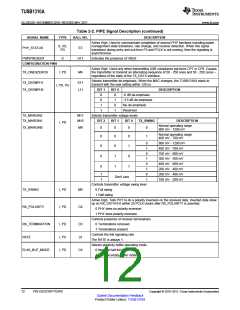
CONTROL AND STATUS SIGNALS
PHY_RESETN
TX_DETRX_LPBK
TX_ELECIDLE
RX_ELECIDLE
I, PU
I, PD
I
J3
M6
K3
F3
Active Low. Resets the transmitter and receiver. This signal is asynchronous.
Active High. Used to tell the PHY to begin a receiver detection operation or to begin
loopback.
Active High. Forces TX output to electrical idle depending on the power state.
S, I/O,
PD
Active High. While de-asserted with the PHY in P0, P1, P2, or P3, indicates detection of
LFPS.
Encodes receiver status and error codes for the received data stream when receiving
data.
RX_STATUS2
C7
O
RX_STATUS1
RX_STATUS0
C6
C5
BIT 2
BIT 1
BIT 0
DESCRIPTION
0
0
0
0
1
1
0
0
1
1
0
0
0
1
0
1
0
1
Received data OK
1 SKP ordered set added
1 SKP ordered set removed
Receiver detected
8B/10B decode error
Elastic buffer overflow
Elastic buffer underflow.
1
1
1
1
0
1
This error code is not used if the elasticity buffer is
operating in the nominal buffer empty mode.
Receive disparity error
POWER_DOWN1
POWER_DOWN0
G3
H3
Power up and down the transceiver power states.
I
BIT 1
BIT 0
DESCRIPTION
0
0
1
1
0
1
0
1
P0, normal operation
P1, low recovery time latency, power saving state
P2, longer recovery time latency, low power state
P3, lowest power state
When transitioning from P3 to P0, the signaling is asynchronous.
Copyright © 2010–2011, Texas Instruments Incorporated
PIN DESCRIPTIONS
11
Submit Documentation Feedback
Product Folder Link(s): TUSB1310A

 TI [ TEXAS INSTRUMENTS ]