TPS7H5005-SEP, TPS7H5006-SEP, TPS7H5007-SEP, TPS7H5008-SEP
www.ti.com
SLVSGG1 – FEBRUARY 2022
external gate drive solution is recommended. For those controllers that support buck and single ended isolated
applications (TPS7H5005-SEP, TPS7H5006-SEP, and TPS7H5007-SEP), OUTA provides the gate control signal
for the main switch in the topology. For push-pull and full-bridge applications, OUTA and OUTB both provide
control signals for the main primary switches. Note that OUTB is only active when the duty cycle limit is set
to 50% by connecting DCL pin to AVSS, and this DCL option is only valid for TPS7H5005-SEP and TPS7H5008-
SEP (see Duty Cycle Programmability for more details). For the two output controller options, OUTA and OUTB
are not perfectly matched and will vary based on the COMP voltage in a given switching cycle.
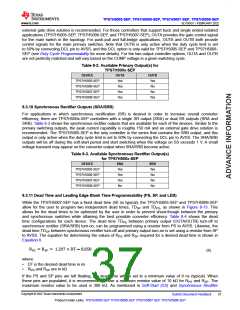
Table 8-2. Available Primary Output(s) for
TPS7H500x-SEP
DEVICE
OUTA
OUTB
Yes
No
TPS7H5005-SEP
TPS7H5006-SEP
TPS7H5007-SEP
TPS7H5008-SEP
Yes
Yes
Yes
No
Yes
Yes
8.3.10 Synchronous Rectifier Outputs (SRA/SRB)
For applications in which synchronous rectification (SR) is desired in order to increase overall converter
efficiency, there are TPS7H500x-SEP controllers with a single SR output (SRA) or dual SR outputs (SRA and
SRB). Table 8-3 shows the synchronous rectifier outputs that are available for each of the devices. Similar to the
primary switching outputs, the peak current capability is roughly 150 mA and an external gate drive solution is
recommended. The TPS7H5005-SEP is the only controller in the series that contains the SRB output, and this
output is only active when the duty cycle limit is set to 50% by connecting the DCL pin to AVSS. The SRA/SRB
outputs will be off during the soft-start period and start switching when the voltage on SS exceeds 1 V. A small
voltage transient may appear on the converter output when SRA/SRB become active.
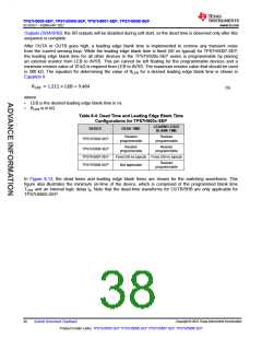
Table 8-3. Available Synchronous Rectifier Output(s)
for TPS7H500x-SEP
DEVICE
SRA
Yes
Yes
Yes
No
SRB
Yes
No
TPS7H5005-SEP
TPS7H5006-SEP
TPS7H5007-SEP
TPS7H5008-SEP
No
No
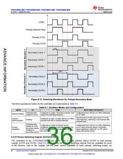
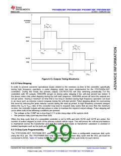
8.3.11 Dead Time and Leading Edge Blank Time Programmability (PS, SP, and LEB)
While the TPS7H5007-SEP has a fixed dead time (50 ns typical), the TPS7H5005-SEP and TPS7H5006-SEP
allow for the user to program two independent dead times, TDSP and TDPS, as shown in Figure 8-13. This
allows for the dead times to be optimized by the user in order to prevent shoot-though between the primary
and synchronous switches while attaining the best possible converter efficiency. Table 8-4 shows the dead
time configurations for each device. The dead time TDPS between primary output (OUTA/OUTB) turn-off to
synchronous rectifier (SRA/SRB) turn-on, can be programmed using a resistor from PS to AVSS. Likewise, the
dead time TDSP between synchronous rectifier turn-off and primary output turn-on is set using a resistor from SP
to AVSS. The equation for determining the values of RPS and RSP required for a desired dead time is shown in
Equation 8.
RPS = RSP = 1.207 × DT 8.858
(8)
where:
•
•
DT is the desired dead time in ns
RPS and RSP are in kΩ
If the PS and SP pins are left floating, the dead time will be set to a minimum value of 8 ns (typical). When
these pins are populated, it is recommended to use a minimum resistor value of 10 kΩ for RPS and RSP. The
maximum resistor value to be used is 300 kΩ. As mentioned in Soft-Start (SS) and Synchronous Rectifier
Copyright © 2022 Texas Instruments Incorporated
Submit Document Feedback
37
Product Folder Links: TPS7H5005-SEP TPS7H5006-SEP TPS7H5007-SEP TPS7H5008-SEP

 TI [ TEXAS INSTRUMENTS ]