TPS55340
www.ti.com
SLVSBD4 –MAY 2012
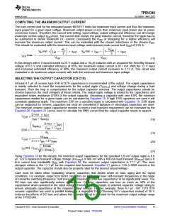
COMPUTING THE MAXIMUM OUTPUT CURRENT
The over-current limit for the integrated power MOSFET limits the maximum input current and thus the maximum
input power for a given input voltage. Maximum output power is less than maximum input power due to power
conversion losses. Therefore, the current limit setting, input voltage, output voltage and efficiency can all change
maximum current output (IOUTmax). The current limit clamps the peak inductor current, therefore the ripple has to
be subtracted to derive maximum DC current. Decreasing the KIND or designing for a higher efficiency will
increase the maximum output current. This can be evaluated with the chosen inductance or the chosen KIND
.
This should be evaluated with the minimum input voltage and minimum peak current limit (ILIM) of 5.25 A.
DIL
KIND
2
æ
ö
÷
ø
æ
ö
÷
ø
V min ´ ILIM
-
´ hEST V min ´ ILIM
´
1-
´ hEST
IN
IN
ç
ç
2
è
è
VOUT
IOUT max =
=
VOUT
(17)
In this design with 5 V input boosted to 24 V output and a 10 μH inductor with an assumed the Schottky forward
voltage of 0.5 V and estimated efficiency of 85%, the maximum output current is 871 mA. With the 12 V input
and increased estimated efficiency of 90%, the maximum output current increases to 2.13 A. This circuit was
evaluated to its maximum output currents with both the minimum and maximum input voltage.
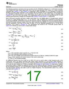
SELECTING THE OUTPUT CAPACITOR (C8-C10)
At least 4.7 µF of ceramic type X5R or X7R capacitance is recommended at the output. The output capacitance
is mainly selected to meet the requirements for the output ripple (VRIPPLE) and voltage change during a load
transient. Then the loop is compensated for the output capacitor selected. The output capacitance should be
chosen based on the most stringent of these criteria. The output ripple voltage is related to the capacitance and
equivalent series resistance (ESR) of the output capacitor. Assuming a capacitor with zero ESR, the minimum
capacitance needed for a given ripple can be calculated by Equation 18. If high ESR capacitors are used it will
contribute additional ripple. The maximum ESR for a specified ripple is calculated with Equation 19. ESR ripple
can be neglected for ceramic capacitors but must be considered if tantalum or electrolytic capacitors are used.
The minimum ceramic output capacitance needed to meet a load transient requirement can be estimated by the
Equation 20. Equation 21 can be used to calculate the RMS current that the output capacitor needs to support.
Dmax ´ IOUT
COUT
³
¦
´ VRIPPLE
SW
(18)
æ
ç
è
ö
÷
ø
Dmax ´ IOUT
V
-
RIPPLE
¦
´ COUT
SW
ESR £
DIL
DITRAN
(19)
(20)
COUT
³
2´ p´ ¦BW ´ DVTRAN
Dmax
ICOrms = IOUT
1- Dmax
(
)
(21)
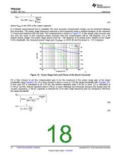
Using Equation 18 for this design, the minimum output capacitance for the specified 120 mV output ripple is 8.8
µF. For a maximum transient voltage change (ΔVTRAN) of 960 mV with a 400 mA load transient (ΔITRAN) and a 6
kHz control loop bandwidth (fBW) with Equation 20, the minimum output capacitance is 11.1 µF. The most
stringent criteria is the 11.1 µF for the required load transient. Equation 21 gives a 1.58 A RMS current in the
output capacitor. The capacitor should also be properly rated for the desired output voltage.
Care must be taken when evaluating ceramic capacitors that derate under dc bias, aging and AC signal
conditions. For example, larger form factor capacitors (in 1206 size) have self-resonant frequencies in the range
of converter switching frequency. Self-resonance causes the effective capacitance to be significantly lower. The
DC bias can also significantly reduce capacitance. Ceramic capacitors can lose as much as 50% of the
capacitance whan operated at the rated voltage. Therefore, allow margin in selected capacitor voltage rating to
ensure adequate capacitance at the required output voltage. For this example, three 4.7 µF, 50V 1210 X7R
ceramic capacitors are used in parallel leading to a negligible ESR. Choosing 50 V capacitors instead of 35 V
reduces the effects of DC bias and allows this example circuit to be rated for the maximum output voltage range
of the TPS55340.
Copyright © 2012, Texas Instruments Incorporated
Submit Documentation Feedback
15
Product Folder Link(s) :TPS55340

 TI [ TEXAS INSTRUMENTS ]