TPS55340
SLVSBD4 –MAY 2012
www.ti.com
SELECTING THE INPUT CAPACITORS (C2, C7)
At least 4.7µF of ceramic input capacitance is recommended. Additional input capacitance may be required to
meet ripple and/or transient requirements. High quality ceramic, type X5R or X7R are recommended to minimize
capacitance variations over temperature. The capacitor must also have an RMS current rating greater than the
maximum RMS input current of the TPS55340 calculated with Equation 22. The input capacitor must also be
rated greater than the maximum input voltage. The input voltage ripple can be calculated with Equation 23.
DIL
ICIrms =
12
(22)
DI
L
4´ ¦SW ´ CIN
Vripple =
+ DIL ´RCIN
I
(23)
In the design example, the input RMS current is calculated to be 191 mA. The chosen input capacitor is a 10 µF,
35V 1210 X7R with 3 mΩ ESR. Although one with a lower voltage rating can be used, a 35 V rated capacitor
was chosen to limit the affects of dc bias and to allow it the circuit to be rated for the entire input range of the
TPS55340. The input ripple is calculated to be 30 mV. An additional 0.1 µF, 50V 0603 X5R is located close to
the VIN and GND pins for extra decoupling.
SETTING OUTPUT VOLTAGE (R1, R2)
To set the output voltage in either DCM or CCM, select the values of R1 and R2 according to the following
equations.
R1
æ
ö
VOUT = 1.229V ´
+1
ç
÷
R2
è
ø
(24)
VOUT
æ
ö
R1= R2´
-1
÷
ç
1.229V
è
ø
(25)
Considering the leakage current through the resistor divider and noise decoupling into FB pin, an optimum value
for R2 is around 10 kΩ. The output voltage tolerance depends on the VFB accuracy and the tolerance of R1 and
R2. In this example with a 24 V output using Equation 25, R1 is calculated to 185.3 kΩ. The nearest standard
value of 187 kΩ is used.
SETTING THE SOFT-START TIME (C7)
Choose the appropriate capacitor to set soft-start time and avoid overshoot. Increasing the soft-start time
reduces the overshoot during start-up. A 0.047 µF ceramic capacitor is used in this example.
SELECTING THE SCHOTTKY DIODE (D1)
The high switching frequency of the TPS55340 demands high-speed rectification for optimum efficiency. Ensure
that the diode’s average and peak current rating exceed the average output current and peak inductor current. In
addition, the diode’s reverse breakdown voltage must exceed the regulated output voltage. The diode must also
be rated for the power dissipated which can be calculated with Equation 26.
PD = VD × IOUT
(26)
In this conservative design example, the diode is chosen to be rated for the maximum output current of 2.13 A.
During normal operation with 800 mA output current and assuming a Schottky diode drop of 0.5V, the diode must
be capable of dissipating 400 mW. The recommended minimum ratings for this design are a 40 V, 3 A diode.
However to improve the flexibility of this design, a Diodes Inc B540-13-F in an SMC package is used with voltage
and current ratings of 40 V and 5A.
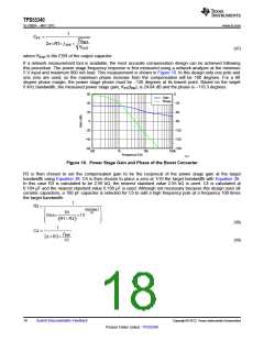
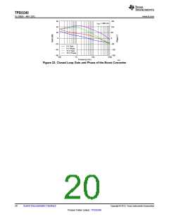
COMPENSATING THE CONTROL LOOP (R3, C4, C5)
The TPS55340 requires external compensation which allows the loop response to be optimized for each
application. The COMP pin is the output of the internal error amplifier. An external resistor R3 and ceramic
capacitor C4 are connected to the COMP pin to provide a pole and a zero, shown in the application circuit. This
pole and zero, along with the inherent pole and zero of a boost converter, determine the closed loop frequency
response. This is important for converter stability and transient response. Loop compensation should be
designed for the minimum operating voltage.
16
Submit Documentation Feedback
Copyright © 2012, Texas Instruments Incorporated
Product Folder Link(s) :TPS55340

 TI [ TEXAS INSTRUMENTS ]