TPS55340
www.ti.com
SLVSBD4 –MAY 2012
DETERMINING THE DUTY CYCLE
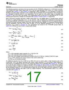
The input to output voltage conversion ratio of the TPS55340 is limited by the worst case maximum duty cycle of
89% and the minimum duty cycle which is determined by the minimum on-time of 77 ns and the switching
frequency. The minimum duty cycle can be estimated with Equation 7. With a 600 kHz switching frequency the
minimum duty cycle is 4%.
DPS = TON min × ƒsw
(7)
The duty cycle at which the converter operates is dependent on the mode in which the converter is running. If the
converter is running in discontinuous conduction mode (DCM), where the inductor current ramps to zero at the
end of each cycle, the duty cycle varies with changes of the load much more than it does when running in
continuous conduction mode (CCM). In continuous conduction mode, where the inductor maintains a minimum
dc current, the duty cycle is related primarily to the input and output voltages as computed below. Assume a 0.5
V drop VD across the Schottky rectifier. At the minimum input of 5 V, the duty cycle will be 80%. At the maximum
input of 12 V, the duty cycle is 51%.
VOUT + VD - V
IN
D =
VOUT + V
D
(8)
At light loads the converter will operate in DCM. In this case the duty cycle is a function of the load, input and
output voltages, inductance and switching frequency as computed below. This can be calculated only after an
inductance is chosen in the following section. While operating in DCM with very light load conditions the duty
cycle demand will force the TPS55340 to operate with the minimum on time. The converter will then begin pulse
skipping which can increase the output ripple.
2´(VOUT + VD - V )´L ´IOUT ´ ¦SW
IN
D =
V
IN
(9)
All converters using a diode as the freewheeling or catch component have a load current level at which they
transit from discontinuous conduction mode to continuous conduction mode. This is the point where the inductor
current just falls to zero during the off-time of the power switch. At higher load currents, the inductor current does
not fall to zero and diode and switch current assume a trapezoidal wave shape as opposed to a triangular wave
shape. The load current boundary between discontinuous conduction and continuous conduction can be found
for a set of converter parameters as follows.
2
V
(
+ VD - V ´ V
IN IN
)
OUT
IOUT(crit)
=
2´ V
(
+ VD 2 ´ ¦SW ´L
)
OUT
(10)
For loads higher than the result of the Equation 10, the duty cycle is given by Equation 8. For loads less than the
results of Equation 10, the duty cycle is given Equation 9. For Equation 7 through Equation 10, the variable
definitions are as follows.
•
•
•
•
•
•
VOUT is the output voltage of the converter in V
VD is the forward conduction voltage drop across the rectifier or catch diode in V
VIN is the input voltage to the converter in V
IOUT is the output current of the converter in A
L is the inductor value in H
ƒSW is the switching frequency in Hz
Unless otherwise stated, the design equations that follow assume that the converter is running in continuous
conduction mode, which typically results in a higher efficiency for the power levels of this converter.
SELECTING THE INDUCTOR (L1)
The selection of the inductor affects steady state operation as well as transient behavior and loop stability. These
factors make it the most important component in power regulator design. There are three important inductor
specifications: inductor value, DC resistance and saturation current. Considering inductor value alone is not
enough. Inductor values can have ±20% tolerance with no current bias. When the inductor current approaches
saturation level, the effective inductance can fall to a fraction of the zero current value.
Copyright © 2012, Texas Instruments Incorporated
Submit Documentation Feedback
13
Product Folder Link(s) :TPS55340

 TI [ TEXAS INSTRUMENTS ]