TPS55340
www.ti.com
SLVSBD4 –MAY 2012
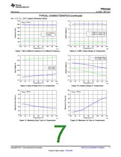
MINIMUM ON TIME AND PULSE SKIPPING
The TPS55340 PWM control system has a minimum PWM pulse width of 77ns (typical). This minimum on-time
determines the minimum duty cycle of the PWM, for any set switching frequency. When the voltage regulation
loop of the TPS55340 requires a minimum on-time pulse width less than 77ns, the IC enters pulse-skipping
mode. In this mode, the device will hold the power switch off for several switching cycles to prevent the output
voltage from rising above the desired regulated voltage. This operation typically occurs in light load conditions
when the PWM operates in discontinuous conduction mode. Pulse skipping increases the output ripple as shown
in Figure 21.
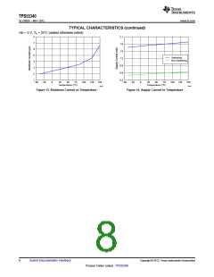
LAYOUT COSIDERATIONS
As for all switching power supplies, especially those with high frequency and high switch current, printed circuit
board (PCB) layout is an important design step. If the layout is not carefully designed, the regulator could suffer
from instability as well as noise problems. To maximize efficiency, switch rise and fall times are made as short as
possible. To prevent radiation of high frequency resonance problems, proper layout of the high frequency
switching path is essential. Minimize the length and area of all traces connected to the SW pin and always use a
ground plane under the switching regulator to minimize inter-plane coupling. The high current path including the
internal MOSFET switch, Schottky diode, and output capacitor, contains nanosecond rise and fall times and
should be kept as short as possible. The input capacitor needs not only to be close to the VIN pin, but also to the
AGND pin in order to reduce the IC supply ripple.
THERMAL CONSIDERATIONS
The maximum IC junction temperature should be restricted to 150°C under normal operating conditions. This
restriction limits the power dissipation of the TPS55340. The TPS55340 features a thermally enhanced QFN
package. This package includes a PowerPad™ that improves the thermal capabilities of the package. The
thermal resistance of the QFN package in any application greatly depends on the PCB layout and the
PowerPad™ connection. The PowerPad™ must be soldered to the analog ground on the PCB. Use thermal vias
underneath the PowerPad™ to achieve good thermal performance.
Copyright © 2012, Texas Instruments Incorporated
Submit Documentation Feedback
11
Product Folder Link(s) :TPS55340

 TI [ TEXAS INSTRUMENTS ]