TPS55340
www.ti.com
SLVSBD4 –MAY 2012
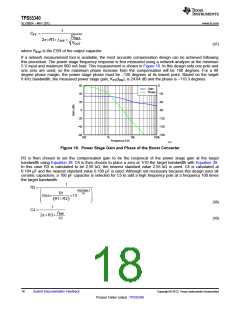
The following equations summarize the loop equations for the TPS55340 configured as a CCM boost converter.
They include the power stage output pole (ƒOUT) and the right-half-plane zero (ƒRHPZ) of a boost converter
calculated with Equation 27 and Equation 28 respectively. When calculating ƒOUT it is important to include the
derating of ceramic output capacitors. In the example with an estimated 10.2 µF capacitance, these frequencies
are calculated to 980 kHz and 22.1 kHz respectively. The DC gain (A) of the power stage is calculated with
Equation 27 and is 39.9 dB in this design. The compensation pole (ƒP) and zero (ƒZ) generated by R3, C4 and
internal transconductance amplifier are calculated with Equation 30 and Equation 31 respectively.
Most CCM boost converters will have a stable control loop if fZ is set slightly above ƒP through proper sizing of
R3 and C4. A good starting point is C4 = 0.1 µF and R3 = 2kΩ. Increasing R3 or reducing C4 increases the
closed loop bandwidth, and therefore improves the transient response. Adjusting R3 and C4 in opposite direction
increases the phase and gain margin of the loop, which improves loop stability. It is generally recommended to
limit the bandwidth of the loop to the lower of either 1/5 of the switching frequency ƒSW or 1/3 the RHPZ
frequency, ƒRHPZ shown in Equation 28. The spreadsheet tool located in the TPS55340 product folder at
www.ti.com can also be used to aid in compensation design.
2
¦
»
OUT
2p´ROUT ´ COUT
(27)
(28)
2
æ
ç
è
ö
÷
ø
ROUT
V
IN
¦
»
´
RHPZ
2p´L
VOUT
V
1.229
VOUT
1
2
IN
A =
´ Gea´10MW ´
´ROUT ´
V
OUT ´RSENSE
(29)
(30)
(31)
(32)
(33)
1
¦
=
P
1
¦
=
Z
¦
SW
¦co1=
¦co2 =
5
¦
RHPZ
3
Where
COUT is the equivalent output capacitor (COUT=C8+C9+C10)
ROUT is the equivalent load resistance (VOUT/IOUT
)
Gea is the error amplifier transconductance located in the ELECTRICAL CHARACTERISTICS table
RSENSE (15mΩ, typical) is the sense resistor in the current control loop
ƒco1 and ƒco2 are possible bandwith.
An additional capacitor from the COMP pin to GND (C5) can be used to place a high frequency pole in the
control loop. This is not always necessary with ceramic output capacitors. If a non-ceramic output capacitor is
used, there is an additional zero (fZESR) in the control loop which can be calculated with Equation 35. The value
of C5 and the pole created by C5 can be calculated with Equation 36 and Equation 34 respectively. Finally if
more phase margin is needed, an additional zero (fZFF) can be added by placing a capacitor (CFF) in parallel with
the top feedback resistor R1. It is recommended to place the zero at the target cross-over frequency or higher.
The feed forward capacitor also adds a pole at a higher frequency. The recommended value of CFF can be
calculated with Equation 37.
1
¦
=
P2
2p´R3´ C5
(34)
1
¦
»
ZESR
2p´RESR ´ COUT
(35)
(36)
R
ESR ´ COUT
C5 =
R3
Copyright © 2012, Texas Instruments Incorporated
Submit Documentation Feedback
17
Product Folder Link(s) :TPS55340

 TI [ TEXAS INSTRUMENTS ]