TPS55340
www.ti.com
SLVSBD4 –MAY 2012
DETAILED DESCRIPTION
OPERATION
The TPS55340 integrates a 5 A, 40 V low side n-channel MOSFET for boost converter output up to 38V. The
TPS55340 regulates the output with current mode PWM (pulse width modulation) control. The PWM control
circuitry turns on the switch at the beginning of each oscillator clock cycle. The input voltage is applied across the
inductor and stores the energy as inductor current ramps up. During this portion of the switching cycle, the load
current is provided by the output capacitor. When the inductor current reaches a threshold level set by the error
amplifier output, the power switch turns off and the external Schottky diode is forward biased to allow the
inductor current to flow to the output. The inductor transfers stored energy to replenish the output capacitor and
supply the load current. This operation repeats every switching cycle. The duty cycle of the converter is
determined by the PWM control comparator which compares the error amplifier output and the current signal.
The oscillator frequency is programmed by the external resistor or synchronized to an external clock signal.
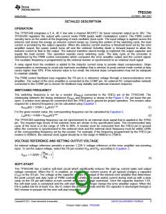
A ramp signal from the oscillator is added to the inductor current ramp to provide slope compensation. Slope
compensation is necessary to avoid sub-harmonic oscillation that is intrinsic to peak current mode control at duty
cycles higher than 50%. If the inductor value is too small, the internal slope compensation may not be adequate
to maintain stability.
The PWM control feedback loop regulates the FB pin to a reference voltage through a transconductance error
amplifier. The output of the error amplifier is connected to the COMP pin. An external RC compensation network
connected to the COMP pin is chosen for feedback loop stability and optimum transient response.
SWITCHING FREQUENCY
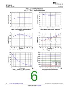
The switching frequency is set by a resistor (RFREQ) connected to the FREQ pin of the TPS55340. The
relationship between the timing resistance RFREQ and frequency is shown in the Figure 5. Do not leave this pin
open. A resistor must always be connected from the FREQ pin to ground for proper operation. The resistor value
required for a desired frequency can be calculated using Equation 1.
RFREQ(kΩ) = 57500 × ƒsw(kHz)–1.03
(1)
For the given resistor value, the corresponding frequency can be calculated by Equation 2.
ƒsw(kHz) = 41600 × RFREQ(kΩ)–0.97
(2)
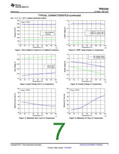
The TPS55340 switching frequency can be synchronized to an external clock signal that is applied to the SYNC
pin. The required logic levels of the external clock are shown in the specification table. The recommended duty
cycle of the clock is in the range of 10% to 90%. A resistor must be connected from the FREQ pin to ground
when the converter is synchronized to the external clock and the external clock frequency must be within ±20%
of the corresponding frequency set by the resistor. For example, if the frequency programmed by the FREQ pin
resistor is 600kHz, the external clock signal should be in the range of 480kHz to 720kHz.
VOLTAGE REFERENCE AND SETTING OUTPUT VOLTAGE
An internal voltage reference provides a precise 1.229 V voltage reference at the error amplifier non-inverting
input. To set the output voltage, select the FB pin resistor RSH and RSL according to Equation 3.
æ
ç
è
ö
RSH
RSL
VOUT = 1.229V ´
+1
÷
ø
(3)
SOFT-START
The TPS55340 has a built-in soft-start circuit which significantly reduces the start-up current spike and output
voltage overshoot. When the IC is enabled, an internal bias current source (6 µA typical) charges a capacitor
(CSS) on the SS pin. The voltage at the capacitor clamps the output of the internal error amplifier that determines
the peak current and duty cycle of PWM controller. Limiting the peak switch current during start-up with a slow
ramp on the SS pin will reduce in-rush current and output voltage overshoot. Once the capacitor reaches 1.8V,
the soft-start cycle is completed and the soft-start voltage no longer clamps the error amplifier output. When the
EN is pulled low for at least 1ms, the IC enters the shutdown mode and the SS capacitor is discharged through a
5kΩ resistor to prepare for the next soft-start sequence.
Copyright © 2012, Texas Instruments Incorporated
Submit Documentation Feedback
9
Product Folder Link(s) :TPS55340

 TI [ TEXAS INSTRUMENTS ]