TPS51211
SLUSAA7 –NOVEMBER 2010
www.ti.com
EXTERNAL COMPONENTS SELECTION
Selecting external components is simple in D-CAP™ mode.
1. Choose the inductor.
The inductance value should be determined to give the ripple current of approximately 1/4 to 1/2 of maximum
output current. Larger ripple current increases output ripple voltage and improves S/N ratio and helps stable
operation.
V
(
- V
´ V
)
V
- V
)
´ V
)
OUT
OUT
OUT
(
IN max
(
OUT
V
IN max
(
IN max
(
)
1
3
L =
´
=
´
I
´ f
V
I
´ f
IND(ripple) SW
SW
IN max
(
OUT max
(
)
)
)
(6)
The inductor also needs to have low DCR to achieve good efficiency, as well as enough room above peak
inductor current before saturation. The peak inductor current can be estimated in Equation 7.
V
(
- VOUT ´ VOUT
)
IN max
(
)
VTRIP
8 ´ RDS(on) L ´ fSW
1
I
=
+
´
IND(peak)
V
IN max
(
)
(7)
2. Choose the output capacitor(s).
Organic semiconductor capacitor(s) or specialty polymer capacitor(s) are recommended. For loop stability,
capacitance and ESR should satisfy Equation 2. For jitter performance, Equation 8 is a good starting point to
determine ESR.
VOUT ´10 mV ´ 1-D
10 mV ´L ´ f
é
ë
ù
û
é
ë
ù
û
(
)
L ´ fSW
SW
ESR =
=
=
W
é ù
ë û
0.7 V ´I
é ù
0.7 V
70
é ù
ë û
IND(ripple)
ë û
where
•
•
•
D is the duty ratio
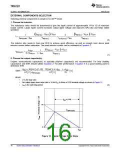
the output ripple down slope rate is 10 mV/tSW in terms of VFB terminal voltage as shown in Figure 15
tSW is the switching period
(8)
t
x (1-D)
SW
10
V
RIPPLE(FB)
0
t
SW
t – Time
Figure 15. Ripple Voltage Down Slope
16
Submit Documentation Feedback
Copyright © 2010, Texas Instruments Incorporated

 TI [ TEXAS INSTRUMENTS ]