TPS51211
SLUSAA7 –NOVEMBER 2010
www.ti.com
LIGHT LOAD CONDITION IN AUTO-SKIP OPERATION
The TPS51211 automatically reduces switching frequency at light load conditions to maintain high efficiency. As
the output current decreases from heavy load condition, the inductor current is also reduced and eventually
comes to the point that its rippled valley touches zero level, which is the boundary between continuous
conduction and discontinuous conduction modes. The rectifying MOSFET is turned off when this zero inductor
current is detected. As the load current further decreases, the converter runs in to discontinuous conduction
mode. The on-time is kept almost the same as it was in the continuous conduction mode so that it takes longer
time to discharge the output capacitor with smaller load current to the level of the reference voltage. The
transition point to the light load operation IO(LL) (i.e., the threshold between continuous and discontinuous
conduction mode) can be calculated in Equation 3.
(V - V
)´ V
OUT
1
IN
OUT
I
=
´
O(LL)
2´L ´ f
V
SW
IN
where
•
fSW is the PWM switching frequency
(3)
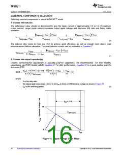
Switching frequency versus output current in the light load condition is a function of L, VIN and VOUT, but it
decreases almost proportional to the output current from the IO(LL) given in Equation 3. For example, it is 58 kHz
at IO(LL)/5 if the frequency setting is 290 kHz.
ADAPTIVE ZERO CROSSING
The TPS51211 has an adaptive zero crossing circuit which performs optimization of the zero inductor current
detection at skip mode operation. This function pursues ideal low-side MOSFET turning off timing and
compensates inherent offset voltage of the ZC comparator and delay time of the ZC detection circuit. It prevents
SW-node swing-up caused by too late detection and minimizes diode conduction period caused by too early
detection. As a result, better light load efficiency is delivered.
OUTPUT DISCHARGE CONTROL
When EN is low, the TPS51211 discharges the output capacitor using internal MOSFET connected between SW
and GND while high-side and low-side MOSFETs are kept off. The current capability of this MOSFET is limited to
discharge slowly.
LOW-SIDE DRIVER
The low-side driver is designed to drive high current low RDS(on) N-channel MOSFET(s). The drive capability is
represented by its internal resistance, which are 1.0Ω for V5IN to DRVL and 0.5Ω for DRVL to GND. A dead time
to prevent shoot through is internally generated between high-side MOSFET off to low-side MOSFET on, and
low-side MOSFET off to high-side MOSFET on. 5-V bias voltage is delivered from V5IN supply. The
instantaneous drive current is supplied by an input capacitor connected between V5IN and GND. The average
drive current is equal to the gate charge at Vgs=5V times switching frequency. This gate drive current as well as
the high-side gate drive current times 5V makes the driving power which need to be dissipated from TPS51211
package.
HIGH-SIDE DRIVER
The high-side driver is designed to drive high current, low RDS(on) N-channel MOSFET(s). When configured as a
floating driver, 5 V of bias voltage is delivered from V5IN supply. The average drive current is also equal to the
gate charge at VGS=5V times switching frequency. The instantaneous drive current is supplied by the flying
capacitor between VBST and SW pins. The drive capability is represented by its internal resistance, which are
1.5 Ω for VBST to DRVH and 0.7 Ω for DRVH to SW.
14
Submit Documentation Feedback
Copyright © 2010, Texas Instruments Incorporated

 TI [ TEXAS INSTRUMENTS ]