TPS51211
www.ti.com
SLUSAA7 –NOVEMBER 2010
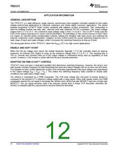
SMALL SIGNAL MODEL
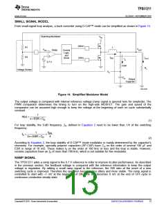
From small-signal loop analysis, a buck converter using D-CAP™ mode can be simplified as shown in Figure 14.
Switching Modulator
V
IN
DRVH
DRVL
R1
R2
L
V
V
OUT
PWM
Control
Logic
and
FB
+
I
I
Driver
IND
OUT
I
+
C
0.7 V
ESR
R
L
Voltage Divider
V
C
C
O
Output
Capacitor
UDG-09063
Figure 14. Simplified Modulator Model
The output voltage is compared with internal reference voltage (ramp signal is ignored here for simplicity). The
PWM comparator determines the timing to turn on the high-side MOSFET. The gain and speed of the
comparator can be assumed high enough to keep the voltage at the beginning of each on cycle substantially
constant.
1
H(s) =
s´ESR ´ C
O
(1)
For loop stability, the 0-dB frequency, ƒ0, defined in Equation 2 need to be lower than 1/4 of the switching
frequency.
f
SW
£
1
f =
0
2p´ESR ´C
4
O
(2)
According to Equation 2, the loop stability of D-CAP™ mode modulator is mainly determined by the capacitor's
chemistry. For example, specialty polymer capacitors (SP-CAP) have CO on the order of several 100 mF and
ESR in range of 10 mΩ. These makes f0 on the order of 100 kHz or less and the loop is stable. However,
ceramic capacitors have an ƒ0 of more than 700 kHz, which is not suitable for this modulator.
RAMP SIGNAL
The TPS51211 adds a ramp signal to the 0.7-V reference in order to improve its jitter performance. As described
in the previous section, the feedback voltage is compared with the reference information to keep the output
voltage in regulation. By adding a small ramp signal to the reference, the S/N ratio at the onset of a new
switching cycle is improved. Therefore the operation becomes less jittery and more stable. The ramp signal is
controlled to start with –7 mV at the beginning of ON-cycle and becomes 0 mV at the end of OFF-cycle in
continuous conduction steady state.
Copyright © 2010, Texas Instruments Incorporated
Submit Documentation Feedback
13

 TI [ TEXAS INSTRUMENTS ]