TPS51211
SLUSAA7 –NOVEMBER 2010
www.ti.com
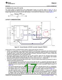
source of the low-side MOSFET through ground. Connect negative node of V5IN capacitor, source of the
low-side MOSFET and GND pad of the device at ground as close as possible. (Refer to loop #3 of
Figure 16)
•
Since the TPS51211 controls output voltage referring to voltage across VOUT capacitor, the top-side resistor of
the voltage divider should be connected to the positive node of VOUT capacitor. In a same manner both
bottom side resistor and GND pad of the device should be connected to the negative node of VOUT capacitor.
The traceꢀfrom these resistors to the VFB pin should be short and thin. Place on the component side and
avoid via(s) between these resistors and the device.
•
•
•
•
Connect the overcurrent setting resistors from TRIP pin to ground and make the connections as close as
possible to the device. The trace from TRIP pin to resistor and from resistor to ground should avoid coupling
to a high-voltage switching node.
Connect the frequency setting resistor from TST pin to ground, or to the PGOOD pin, and make the
connections as close as possible to the device. The trace from the TST pin to the resistor and from the
resistor to ground should avoid coupling to a high-voltage switching node.
Connections from gate drivers to the respective gate of the high-side or the low-side MOSFET should be as
short as possible to reduce stray inductance. Use 0.65 mm (25 mils) or wider traceꢀand via(s) of at least
0.5 mm (20 mils) diameter along this trace.
The PCB trace defined as switch node, which connects to source of high-side MOSFET, drain of low-side
MOSFET and high-voltage side of the inductor, should be as short and wide as possible.
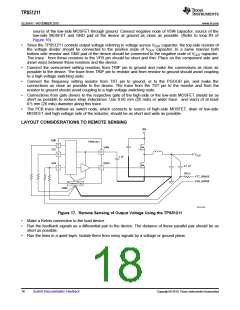
LAYOUT CONSIDERATIONS TO REMOTE SENSING
VIN
TRIP
TPS51211
2
V5IN
TST
6
5
V
OUT
1 mF
VFB
DRVL
0.1 mF
100 W
4
5
VTT_SENSE
VSS_SENSE
Thermal Pad
GND
UDG-10163
Figure 17. Remote Sensing of Output Voltage Using the TPS51211
Make a Kelvin connection to the load device.
Run the feedback signals as a differential pair to the device. The distance of these parallel pair should be as
short as possible.
•
•
•
Run the lines in a quiet layer. Isolate them from noisy signals by a voltage or ground plane.
18
Submit Documentation Feedback
Copyright © 2010, Texas Instruments Incorporated

 TI [ TEXAS INSTRUMENTS ]