TPS51211
SLUSAA7 –NOVEMBER 2010
www.ti.com
APPLICATION INFORMATION
GENERAL DESCRIPTION
The TPS51211 is a high-efficiency, single channel, synchronous buck regulator controller suitable for low output
voltage point-of-load applications in notebook computers and similar digital consumer applications. The device
features proprietary D-CAP™ mode control combined with adaptive on-time architecture. This combination is
ideal for building modern low duty ratio, ultra-fast load step response DC-DC converters. The output voltage
ranges from 0.7 V to 2.6 V. The conversion input voltage range is from 3 V to 28 V. The D-CAP™ mode uses the
ESR of the output capacitor(s) to sense current information. An advantage of this control scheme is that it does
not require an external phase compensation network, helping the designer with ease-of-use and realizing low
external component count configuration. Adaptive on-time control tracks the preset switching frequency over a
wide range of input and output voltages, while it increases the switching frequency at step-up of load.
The strong gate drivers of the TPS51211 allow low RDS(on) FETs for high-current applications.
ENABLE AND SOFT START
When the EN pin voltage rises above the enable threshold, (typically 1.2 V) the controller enters its start-up
sequence. An internal DAC begins to ramp up the reference voltage from 0 V to 0.7 V. This ramping time is
750 ms. Smooth and constant ramp up of the output voltage is maintained during start up regardless of load
current. Connect a 1-kΩ resistor in series with the EN pin to provide protection.
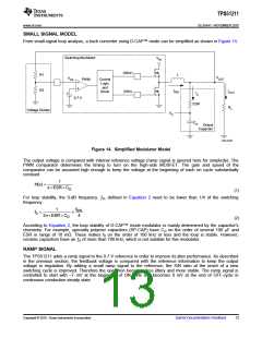
ADAPTIVE ON-TIME D-CAP™ CONTROL
TPS51211 does not have a dedicated oscillator that determines switching frequency. However, the device runs
with pseudo-constant frequency by feed-forwarding the input and output voltages into its on-time one-shot timer.
The adaptive on-time control adjusts the on-time to be inversely proportional to the input voltage and proportional
to the output voltage (tON ∝ VOUT / VIN ). This makes the switching frequency fairly constant in steady state
conditions over wide input voltage range.
The off-time is modulated by a PWM comparator. The VFB node voltage (the mid point of resistor divider) is
compared to the internal 0.7-V reference voltage added with a ramp signal. When both signals match, the PWM
comparator asserts the set signal to terminate the off-time (turn off the low-side MOSFET and turn on high-side
MOSFET). The set signal becomes valid if the inductor current level is below OCP threshold, otherwise the
off-time is extended until the current level to become below the threshold.
12
Submit Documentation Feedback
Copyright © 2010, Texas Instruments Incorporated

 TI [ TEXAS INSTRUMENTS ]