TPS51211
www.ti.com
SLUSAA7 –NOVEMBER 2010
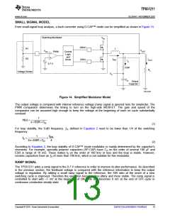
3. Determine the value of R1 and R2.
The output voltage is programmed by the voltage-divider resistor, R1 and R2, shown in Figure 14. R1 is
connected between the VFB pin and the output, and R2 is connected between the VFB pin and GND. Typical
designs begin with the selection of an R2 value between 10 kΩ and 20 kΩ. Determine R1 using Equation 9.
I
´ESR
æ
ö
IND(ripple)
V
-
- 0.7
ç
ç
÷
÷
OUT
2
è
ø
R1=
´R2
0.7
(9)
LAYOUT CONSIDERATIONS
VIN
TRIP
2
TPS51211
V5IN
TST
5
V
OUT
6
5
# 1
1 mF
# 2
VFB
4
DRVL
Thermal Pad
GND
# 3
UDG-10162
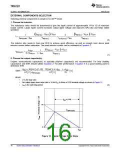
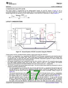
Figure 16. Ground System of DC/DC Converter Using the TPS51211
Certain points must be considered before starting a layout work using the TPS51211.
•
Inductor, VIN capacitor(s), VOUT capacitor(s) and MOSFETs are the power components and should be placed
on one side of the PCB (solder side). Other small signal components should be placed on another side
(component side). At least one inner plane should be inserted, connected to ground, in order to shield and
isolate the small signal traces from noisy power lines.
•
•
All sensitive analog traces and components such as VFB, PGOOD, TRIP and TST should be placed away
from high-voltage switching nodes such as SW, DRVL, DRVH or VBST toꢀavoid coupling. Use internal
layer(s) as ground plane(s) and shield feedback trace from power traces andꢀcomponents.
The DC/DC converter has several high-current loops. The area of these loops should be minimized in order to
suppress generating switching noise.
–
The most important loop to minimize the area of is the path from the VIN capacitor(s) through the high and
low-side MOSFETs, and back to the capacitor(s) through ground. Connect the negative node of the VIN
capacitor(s) and the source of the low-side MOSFET at ground as close as possible. (Refer to loop #1 of
Figure 16)
–
–
The second important loop is the path from the low-side MOSFET through inductor and VOUT capacitor(s),
and back to source of the low-side MOSFET through ground. Connect source of the low-side MOSFET
and negative node of VOUT capacitor(s) at ground as close as possible. (Refer to loop #2 of Figure 16)
The third important loop is of gate driving system for the low-side MOSFET. To turn on the low-side
MOSFET, high current flows from V5IN capacitor through gate driver and the low-side MOSFET, and back
to negative node of the capacitor through ground. To turn off the low-side MOSFET, high current flows
from gate of the low-side MOSFET through the gate driver and GND pad of the device, and back to
Copyright © 2010, Texas Instruments Incorporated
Submit Documentation Feedback
17

 TI [ TEXAS INSTRUMENTS ]