TPS51640A, TPS59640, TPS59641
SLUSAQ2 –JANUARY 2012
www.ti.com
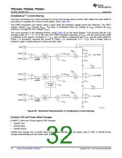
Gate Driver
The TPS51640A, TPS59640, and TPS59641 incorporate two internal strong, high-performance gate drives with
adaptive cross-conduction protection. These drivers are for two phases in the CPU channel. The third phase of
the CPU and the single-phase GPU channel require external drivers.
The internal driver in these devices uses the state of the CDLx and CSWx pins to be sure the high-side or
low-side FET is OFF before turning the other ON. Fast logic and high drive currents (up to 8-A typical) quickly
charge and discharge FET gates to minimize dead-time to increase efficiency. The high-side gate driver also
includes an integrated boost FET instead of merely a diode to increase the effective drive voltage for higher
efficiency. A zero-crossing detection logic, which detects the switch-node voltage before turning OFF the low-side
FET, is used to minimize losses during DCM operation.
Input Under Voltage Protection (5V and 3.3V)
The TPS51640A, TPS59640, and TPS59641 continuously monitor the voltage on the V5DRV, V5 and V3R3 pin
to be sure the value is high enough to bias the device properly and provide sufficient gate drive potential to
maintain high efficiency. The converter starts with approximately 4.4-V and has a nominal 200 mV of hysteresis.
The input (VBAT) does not have a UVLO function, so the circuit operates with power inputs as low as
approximately 3 x VCORE
.
Power Good (CPGOOD and GPGOOD)
These devices have two open-drain power good pins that follow the requirements for IMVP-7. CPGOOD is used
for the CPU channel output voltage and GPGOOD is used for the GPU channel output voltage. Both of these
signals are active high. The upper and the lower limits for the output voltage for xPGOOD active are:
•
•
Upper: VDAC +220 mV
Lower : VDAC –315 mV
xPGOOD goes inactive (low) as soon as the VR_ON pin is pulled low or an undervoltage condition on V5 or
V3R3 is detected. The xPGOOD signals are masked during DAC transitions to prevent false triggering during
voltage slewing.
Output Under Voltage Protection
Output undervoltage protection works in conjunction with the current protection described below. If VCORE drops
below the low PGOOD threshold, then the drivers are turned OFF until VR_ON is cycled.
Overcurrent Protection
The TPS51640A, TPS59640, and TPS59641 use a valley current limiting scheme, so the ripple current must be
considered. The DC current value at OCP is the OCP limit value plus half of the ripple current. Current limiting
occurs on a phase-by-phase and pulse-by-pulse basis. If the voltage between xCSPx and xCSNx is above the
OCP value, the converter delays the next ON pulse until it drops below the OCP limit. For inductor current
sensing circuits, the voltage between xCSPx and xCSNx is the inductor DCR value multiplied by the resistor
divider which is part of the NTC compensation network. As a result, a wide range of OCP values can be obtained
by changing the resistor divider value. In general, use the highest OCP setting possible with the least attenuation
in the resistor divider to provide as much signal to the device as possible. This provides the best performance for
all parameters related to current feedback.
In OCP mode, the voltage drops until the UVP limit is reached. Then, the converter sets the xPGOOD to inactive,
and the drivers are turned OFF. The converter remains in this state until the device is reset by the VR_ON.
Overvoltage Protection
An OVP condition is detected when VCORE is more than 220 mV greater than VDAC. In this case, the converter
sets xPGOOD inactive, and turns ON the drive for the Low-side FET. The converter remains in this state until the
device is reset by cycling VR_ON. However, because of the dynamic nature of IMVP-7 systems, the +220 mV
OVP threshold is blanked much of the time. In order to provide protection to the processor 100% of the time,
there is a second OVP level fixed at 1.7 V which is always active. If the fixed OVP condition is detected, the
PGOOD are forced inactive and the low-side FETs are tuned ON. The converter remains in this state until
VR_ON is cycled.
36
Submit Documentation Feedback
Copyright © 2012, Texas Instruments Incorporated

 TI [ TEXAS INSTRUMENTS ]