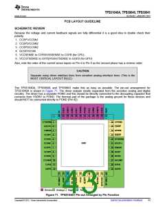
TPS51640A, TPS59640, TPS59641
www.ti.com
SLUSAQ2 –JANUARY 2012
DESIGN STEPS
The design procedure using the TPS51640A, TPS59640, and TPS59641 is very simple . An excel-based
component value calculation tool is available. Contact your local TI representative to get a copy of the
spreadsheet.
The procedure is explained here below with the following design example:
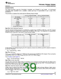
CPU VCORE SPECIFICATIONS
GFX VCORE SPECIFICATIONS
No. of phases
Input Voltage Range
VHFM
3
9 V to 20 V
0.9 V
1
9 V to 20 V
1.23 V
33 A
ICC(max)
94 A
IDYN-MAX
66 A
20 A
ICC-TDC
52
21.5
Load-line
1.9 mV/A
10 mV/µs
3.9 mV/A
10 mV/µs
Fast Slew Rate (minimum)
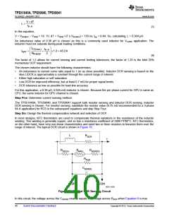
Step One: Select Switching Frequency.
The CPU channel switching frequency is selected by a resistor from CF-IMAX to GND (RCF) and GPU channel
switching frequency is selected by a resistor from GF-IMAX to GND (RGF). The frequency is an approximate
frequency and is expected to vary based on load and input voltage.
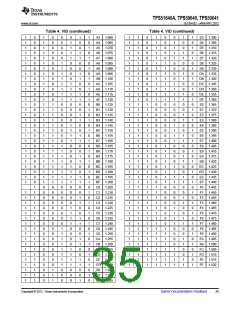
CPU CHANNEL FREQUENCY
(kHz)
GPU CHANNEL FREQUENCY
(kHz)
SELECTION RESISTANCE (kΩ)
20
24
250
300
350
400
450
500
550
600
275
330
385
440
495
550
605
660
30
39
56
75
100
150
For this design, the switching frequency for CPU channel is chosen to be 300 kHz and GPU channel is chosen to
be 385 kHz. Therefore,
RCF = 24 kΩ and RGF = 30 kΩ
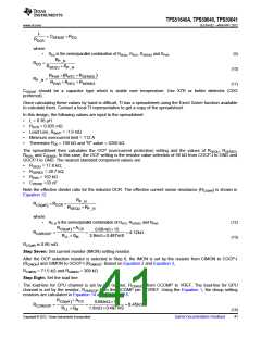
Step Two: Set ICC(max)
The ICC(max) is set by the voltage on CF-IMAX for CPU channel and GF-IMAX for GPU channel. This is set by the
resistors from VREF to CF-IMAX (RCMAX) and from VREF to GF-IMAX (RGMAX
)
From Equation 4 and Equation 5,
RCMAX = 42.2 kΩ and RGMAX = 200 kΩ.
Step Three: Set the Slew Rate
The slew rate is set by the voltage setting on SLEWA pin. For a minimum 10 mV/ms slew rate, the voltage on the
SLEWA pin must be: 0.8 V. This is set by a resistor divider on SLEWA pin from VREF. The low-side resistor is
chosen to be 150 kΩ and the high-side resistor is calculated as 169 kΩ.
Step Four: Determine inductor value and choose inductor.
Smaller values of inductor have better transient performance but higher ripple and lower efficiency. Higher values
have the opposite characteristics. It is common practice to limit the ripple current to 20% to 40% of the maximum
current per phase. In this case, we use 30%:
94A
I
=
´ 0.3 = 9.4A
P-P
3
(6)
39
Copyright © 2012, Texas Instruments Incorporated
Submit Documentation Feedback

 TI [ TEXAS INSTRUMENTS ]