TPS51285A
TPS51285B
SLVSBX0 –APRIL 2013
www.ti.com
Output Overvoltage and Undervoltage Protection
TPS51285A and TPS51285B assert the overvoltage protection (OVP) when VFBx voltage reaches OVP trip
threshold level. When an OVP event is detected, the controller changes the output target voltage to 0 V. This
usually turns off DRVH and forces DRVL to be on. When the inductor current begins to flow through the low-side
MOSFET and reaches the negative OCL, DRVL is turned off and DRVH is turned on. After the on-time expires,
DRVH is turned off and DRVL is turned on again. This action minimizes the output node undershoot due to LC
resonance. When the VFBx reaches 0 V, the driver output is latched as DRVH off and DRVL on. The
undervoltage protection (UVP) latch is set when the VFBx voltage remains lower than UVP trip threshold voltage
for 250 μs or longer. In this fault condition, the controller latches DRVH low and DRVL low and discharges the
outputs through VO1(CH1) and SW2 (CH2). UVP detection function is enabled after 1.1 ms of SMPS operation
to ensure startup. Toggle ENx to clear the fault latch.
Undervoltage Lockout (UVLO) Protection
TPS51285A and B have undervoltage lock out protection at VIN, VREG5 and VREG3. When each voltage is
lower than their UVLO threshold voltage, both SMPS are shut-off. They are non-latch protections.
Over-Temperature Protection
TPS51285A and TPS51285B features an internal temperature monitor. If the temperature exceeds the threshold
value (typically 140°C), the device is shut off including LDOs. This is non-latch protection.
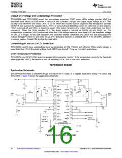
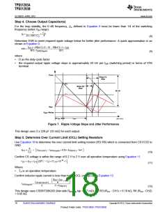
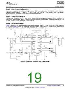
REFERENCE DESIGN
Application Schematic
This session describes a simplified design procedure for 5 V and 3.3 V outputs application using TPS1285A and
TPS1285B. Figure 6 shows the application schematic.
VIN
C2
U1
C1
12 VIN
C8
R7
C7
R8
Q1
17 VBST1
16 DRVH1
18 SW1
VBST2
DRVH2 10
SW2
9
Q2
R9
L1
L2
R10
VOUT
3.3 V
VOUT
5 V
8
C4
C3
15 DRVL1
14 VO1
DRVL2 11
R1
R2
2
1
VFB1
CS1
VFB2
CS2
4
5
7
6
3
R3
R4
R6
PGOOD
EN2
PGOOD
EN 3.3 V
19 VCLK
20 EN1
EN 5V
VREG3
(3.3-V LDO)
VREG3
GND
VREG5
(5-V LDO)
13 VREG5
R5
Thermal-Pad
C5
C6
R11
Figure 6. Application Schematic
16
Submit Documentation Feedback
Copyright © 2013, Texas Instruments Incorporated
Product Folder Links: TPS51285A TPS51285B

 TI [ TEXAS INSTRUMENTS ]