TPS51285A
TPS51285B
www.ti.com
SLVSBX0 –APRIL 2013
Step 6. Select Decoupling Capacitors
Use ceramic capacitors with a value of 4.7 µF or larger (X5R grade or better) for C5 (VREG5) and C6 (VREG3).
For the VIN input capacitors (C1 and C2), 2 x 10 µF (1206, 25V, X5R) MLCC per channel is used in the design.
Tighter tolerances and higher voltage ratings are always appreciated.
Step 7. Peripheral Components
For high-side N-channel MOSFET drive circuit, connect boot strap capacitor between VBSTx and SWx. To
control gate driver strength, adding a resistor (reserved space) is recommended. This design uses 0.1 µF (C7
and C8), 0 Ω (R7 and R8), 6.8 Ω (R9) and 8.2 Ω (R10).
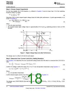
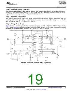
Step 8. Charge Pump Design
Figure 6 shows a circuit design without an external charge pump. Add R11 = 200Ω from VCLK to GND to disable
VCLK signal. Figure 8 shows the design with an external charge pump. D1 (4-in 1 Diode: BAS40DW-04) should
be tied to the 5V switcher output and 4 x 0.1 µF (C9, C10, C11 and C12) is used.
VIN
C2
U1
C1
12 VIN
C8
R7
C7
R8
Q1
17 VBST1
16 DRVH1
18 SW1
VBST2
DRVH2 10
SW2
9
Q2
R9
L1
L2
R10
VOUT
3.3 V
VOUT
5 V
8
C4
C3
15 DRVL1
14 VO1
DRVL2 11
R1
R2
2
1
VFB1
CS1
VFB2
CS2
4
5
7
6
3
R3
R4
R6
PGOOD
EN2
PGOOD
EN 3.3 V
19 VCLK
20 EN1
C11
C12
D1
EN 5V
VREG3
(3.3-V LDO)
Charge-pump
Output
VREG3
GND
VREG5
(5-V LDO)
13 VREG5
R5
Thermal-Pad
C5
C6
C10
C9
Figure 8. Application Schematic (with Charge pump)
Copyright © 2013, Texas Instruments Incorporated
Submit Documentation Feedback
19
Product Folder Links: TPS51285A TPS51285B

 TI [ TEXAS INSTRUMENTS ]