TPS51285A
TPS51285B
www.ti.com
SLVSBX0 –APRIL 2013
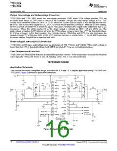
Soft-Start and Discharge
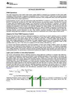
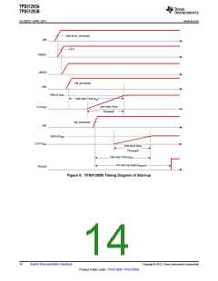
The TPS51285A and TPS51285B operates an internal, 0.8-ms, voltage servo soft-start for each channel. When
the ENx pin becomes higher than the enable threshold voltage, an internal DAC begins ramping up the reference
voltage to the target (2 V). Smooth control of the output voltage is maintained during start-up. When ENx
becomes lower than the lower level of threshold voltage, the device discharges outputs using internal MOSFETs
through VO1 (CH1) and SW2 (CH2).
VREG5 and VREG3 Linear Regulators
There are two 100-mA standby linear regulators that output 5 V and 3.3 V, respectively. The VREG5 provides
the current for gate drivers. VREG3ꢀfunctions as the main power supply for the analog circuitry of the device.
A ceramic capacitor with a value of 4.7 µF or larger (X5R grade or better) is required for each of VREG5 and
VREG3. It should be placed close to the VREG5 pin and the VREG3 pin respectively to stabilize the LDOs.
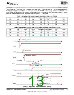
The VREG5 pin switchover function is asserted when three conditions are present:
•
•
•
CH1 is not in UVP/OVP condition
CH1 is not in OCL condition
VO1 voltage is higher than (VREG5 -1V)
In this switchover condition three things occur:
•
•
•
the internal 5-V LDO regulator is shut off
the VREG5 output is connected to VO1 by internal switchover MOSFET
VREG3 input pass is changed from VIN to VO1
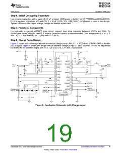
VCLK for Charge Pump
A 256 kHz VCLK signal can be used for the external charge pump circuit. The VCLK signal becomes available
when EN1 enters ON state. VCLK driver circuit is driven by VO1 voltage. In a design that does not require VCLK
output, tie 200 Ω between VCLK pin and GND so that VCLK is turned off.
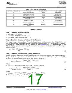
Overcurrent Protection
TPS51285A and TPS51285B have cycle-by-cycle over current limiting control. The inductor current is monitored
during the OFF state and the controller maintains the OFF state during the inductor current is larger than the
overcurrent trip level. In order to provide both good accuracy and cost effective solution, the device supports
temperature compensated MOSFET RDS(on) sensing. The CSx pin should be connected to GND through the CS
voltage setting resistor, RCS. The CSx pin sources CS current (ICS) which is 50 µA typically at room temperature,
and the CSx terminal voltage (VCS= RCS × ICS) should be in the range of 0.2 V to 2 V over all operation
temperatures.ꢀThe trip level is set to the OCL trip voltage (VTRIP) as shown in Equation 3.
R
´I
CS CS
V
=
+1mV
TRIP
8
(3)
The inductor current is monitored by the voltage between GND pin and SWx pin so that SWx pin should be
connected to the drain terminal of the low-side MOSFET properly.The CS pin current has a 4500 ppm/°C
temperature slope to compensate the temperature dependency of the RDS(on). GND is used as the positive
current sensing node so that GND should be connected to the source terminal of the low-side MOSFET.
As the comparison is done during the OFF state, VTRIP sets the valley level of the inductor current. Thus, the load
current at the overcurrent threshold, IOCL(DC), can be calculated as shown in Equation 4.
I
V
IN - VOUT ´ V
IND ripple
(
(
)
VTRIP
VTRIP
)
1
OUT
IOCL(DC)
=
+
=
+
´
RDS on
2
RDS on
2´L ´ fSW
V
IN
( )
( )
(4)
In an overcurrent condition, the current to the load exceeds the current to the output capacitor thus the output
voltage tends to fall down. Eventually, it ends up with crossing the undervoltage protection threshold and
shutdown both channels.
Copyright © 2013, Texas Instruments Incorporated
Submit Documentation Feedback
15
Product Folder Links: TPS51285A TPS51285B

 TI [ TEXAS INSTRUMENTS ]