TPS51285A
TPS51285B
www.ti.com
SLVSBX0 –APRIL 2013
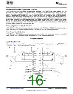
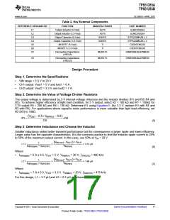
Table 3. Key External Components
REFERENCE DESIGNATOR
FUNCTION
MANUFACTURER
PART NUMBER
L1
L2
Output Inductor (5-Vout)
Output Inductor (3.3-Vout)
Output Capacitor (5-Vout)
Output Capacitor (3.3-Vout)
MOSFET (5-Vout)
ALPS
ALPS
SANYO
SANYO
TI
GLMC3R303A
GLMC2R203A
C3
C4
Q1
Q2
C5
6TPS220MAZB x 2
6TPS220MAZB x 2
CSD87330Q3D
MOSFET (3.3-Vout)
TI
CSD87330Q3D
Decoupling Capacitance
(VREG5)
MURATA
GRM188B30J475ME84
C6
Decoupling Capacitance
(VREG3)
MURATA
GRM188B30J475ME84
Design Procedure
Step 1. Determine the Specifications:
•
•
•
VIN range = 5.5 V to 20 V
CH1 output: Vout1 = 5 V and Iout1 = 6 A
CH2 output: Vout2 = 3.3 V and Iout2 = 7 A
Step 2. Determine the Value of Voltage Divider Resistors
The output voltage is determined by 2-V internal voltage reference and the resistor dividers (R1 and R2/ R4 and
R5). To achieve higher efficiency at light load condition, for 5 V output, select R2 = 100 kΩ and R1 = 150kΩ for
3.3V output R5 = 200 kΩ and R4 = 130 kΩ. Determine R1 using Equation 5. (for 3.3 V, replace R1 with R4 and
R2 with R5). For applications where signal-to-noise performance is more valuable than light load efficiency, set
R2 (R5) to 10kΩ.
V
(
- 0.5´ V
- 2.0
)
OUT
RIPPLE
R1=
´R2
2.0
(5)
Step 3. Determine Inductance and Choose the Inductor
Smaller inductance yields better transient performance but the consequence is larger ripple and lower efficiency.
Larger value has the opposite characteristics. It is the common practice to limit the inductor ripple current to 25%
to 50% of the maximum output current. In this case, use 50% at VIN = 20 V.
V
(
IN(max)
- V
× V
OUT OUT
)
1
L1 =
×
= 3.13 mH
I
× f
V
IND(ripple)
SW(CH1)
IN(max)
(6)
Where
IIND(ripple) = 6 A x 0.5, VOUT = 5 V. VIN(MAX) = 20 V, ƒSW(CH2) = 400 kHz
•
V
(
IN(max)
- V
× V
OUT OUT
)
1
L2 =
×
= 1.66 mH
I
× f
V
IND(ripple)
SW(CH2)
IN(max)
(7)
Where
IIND(ripple) = 7 A x 0.5, VOUT = 3.3 V. VIN(MAX) = 20 V, ƒSW(CH2) = 475 kHz
•
For this design, L1 = 3.3 µH and L2 = 2.2 µH are chosen.
Copyright © 2013, Texas Instruments Incorporated
Submit Documentation Feedback
17
Product Folder Links: TPS51285A TPS51285B

 TI [ TEXAS INSTRUMENTS ]