TPS51285A
TPS51285B
SLVSBX0 –APRIL 2013
www.ti.com
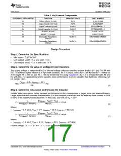
Step 4. Choose Output Capacitor(s)
For the loop stability, the 0 dB frequency, ƒ0, defined in Equation 8 must be lower than 1/4 of the switching
frequency (entire VIN range).
f
sw
£
1
f
=
0
2p ´ ESR ´ C
4
O
(8)
Determine ESR to meet required ripple voltage below for better jitter performance. A quick approximation is as
shown in Equation 9.
V
´ 20[mV ]´ (1- D) 20[mV ]´ L ´ f
SW
=
OUT
ESR =
2[V ]´ I
2[V ]
IND(Ripple)
(9)
where
•
•
D as the duty-cycle factor
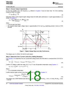
the required output ripple voltage slope is approximately 20 mV per tSW (switching period) in terms of VFB
terminal
V
VOUT
Slope (1)
Jitter
(2)
(1)
Slope (2)
Jitter
20 mV
V
REF
V
+Noise
REF
t
ON
t
OFF
UDG-12012
Figure 7. Ripple Voltage Slope and Jitter Performance
This design uses 2 x 220 µF (35 mΩ) for each output.
Step 5. Determine Over Current Limit (OCL) Setting Resistors
Use Equation 10 to determine the over current limit setting resistor (R3/ R6) which is connected from CS1/CS2 to
GND.
8
é
ù
´ 0.5)´ R -1mV
DS(ON)
R
=
´
(I
- I
IND(ripple)
CS
OCL(DC)
ë
û
I
CS
(10)
(11)
Confirm CS voltage is within the range of 0.2 V to 2 V over all operation temperature using Equation 11.
o
-6
é
ù
V
= R ´ I
CS
(25 C - T )´TC ´10 + 1
CS
CS
A
CS
ê
ë
ú
û
Where
TA is an operation temperature
Confirm inductor ripple current is less than half of OCL (valley) using Equation 12
•
R
´ I
æ
ö
CS
CS
+ 1mV
ç
÷
I
8
OCL(VALLEY )
è
ø
I
<
=
IND(ripple)
2
2´ R
DS(ON)
(12)
This design uses CSD87330Q3D (low-side RDS(ON) typ = 4.7 mΩ) and R3 (RCS - CH1) = 6.19 kΩ, R6 (RCS - CH2)
= 6.65 kΩ.
18
Submit Documentation Feedback
Copyright © 2013, Texas Instruments Incorporated
Product Folder Links: TPS51285A TPS51285B

 TI [ TEXAS INSTRUMENTS ]