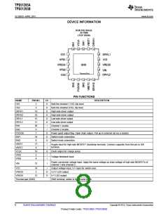
TPS51285A
TPS51285B
www.ti.com
SLVSBX0 –APRIL 2013
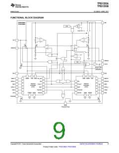
DETAILED DESCRIPTION
PWM Operations
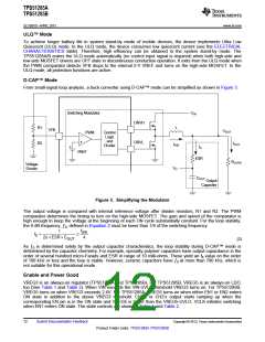
The main control loop of the switch mode power supply (SMPS) is designed as an adaptive on-time pulse width
modulation (PWM) controller. It supports a proprietary D-CAP™ mode. D-CAP™ mode does not require external
compensation circuits and is suitable for low external component count configuration when used with appropriate
amount of ESR at the output capacitor(s).
At the beginning of each cycle, the synchronous high-side MOSFET is turned on, or enters the ON state. This
MOSFET is turned off, or enters the ‘OFF state, after the internal, one-shot timer expires. The MOSFET is turned
on again when the feedback point voltage, VVFB, decreased to match the internal 2-V reference. The inductor
current information is also monitored and should be below the overcurrent threshold to initiate this new cycle. By
repeating the operation in this manner, the controller regulates the output voltage. The synchronous low-side
(rectifying) MOSFET is turned on at the beginning of each OFF state to maintain a minimum of conduction loss.
The low-side MOSFET is turned off before the high-side MOSFET turns on at next switching cycle or when the
detecting inductor current decreases to zero. This enables seamless transition to the reduced frequency
operation during light-load conditions so that high efficiency is maintained over a broad range of load current.
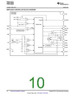
Adaptive On-Time/ PWM Frequency Control
Because the device does not have a dedicated oscillator for control loop on board, switching cycle is controlled
by the adaptive on-time circuit. The on-time is controlled to meet the target switching frequency by feed-
forwarding the input and output voltage into the on-time one-shot timer. To achieve higher duty operation for
lower input voltage application (2-cell battery), the target switching frequency is varied according to the input
voltage. The switching frequency of CH1 (5-V output) is 400kHz during continuous conduction mode (CCM)
operation when VIN = 20 V. The CH2 (3.3-V output) is 475 kHz during CCM when VIN = 20 V.
To improve load transient performance and load regulation in lower input voltage condition, device can extend
the on-time. The maximum on-time extension of CH1 is 5 times. For CH2, it is 2 times. To maintain a reasonable
inductor ripple current during on-time extension, the inductor ripple current should be set to less than half of the
OCL (valley) threshold. The on-time extension function provides high duty cycle operation and shows better DC
(static) performance. AC performance is determined mostly by the output LC filter and resistive factor in the loop.
Light Load Condition in Auto-Skip Operation
The device automatically reduces switching frequency during light-load conditions to maintain high efficiency.
This reduction of frequency is achieved smoothly. A more detailed description of this operation is as follows. As
the output current decreases from heavy-load condition, the inductor current is also reduced and eventually
approaches valley zero current, which is the boundary between continuous conduction mode and discontinuous
conduction mode. The rectifying MOSFET is turned off when this zero inductor current is detected. As the load
current further decreases, the converter runs in discontinuous conduction mode and it takes longer and longer to
discharge the output capacitor to the level that requires the next ON cycle. In reverse, when the output current
increase from light load to heavy load, the switching frequency increases to the preset value as the inductor
current reaches to the continuous conduction. The transition load point to the light load operation IOUT(LL) (that is,
the threshold between continuous and discontinuous conduction mode) can be calculated as shown in n
Equation 1.
V
- V
´ V
(
)
OUT OUT
V
IN
1
IN
I
=
´
OUT LL
( )
2´L ´ f
SW
where
•
fSW is the PWM switching frequency
(1)
Switching frequency versus output current during light-load conditions is a function of inductance (L), input
voltage (VIN) and output voltage (VOUT), but it decreases almost proportional to the output current from the
IOUT(LL)
.
Copyright © 2013, Texas Instruments Incorporated
Submit Documentation Feedback
11
Product Folder Links: TPS51285A TPS51285B

 TI [ TEXAS INSTRUMENTS ]