TPS43060
TPS43061
SLVSBP4A –DECEMBER 2012–REVISED DECEMBER 2012
www.ti.com
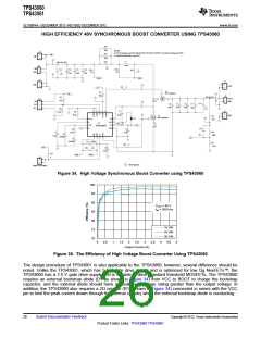
HIGH EFFICIENCY 40V SYNCHRONOUS BOOST CONVERTER USING TPS43060
Figure 34. High Voltage Synchronous Boost Converter using TPS43060
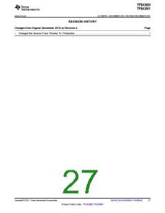
100
95
90
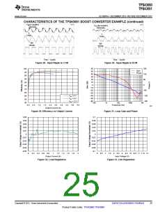
VOUT = 40 V
fsw = 300 kHz
85
80
10 VIN
75
70
24 VIN
38 VIN
0
0.5
1
1.5
2
2.5
3
3.5
4
4.5
5
C001
Output Current (A)
Figure 35. The Efficiency of High Voltage Boost Converter Using TPS43060
The design procedure of TPS43061 is also applicable to the TPS43060; however, several difference should be
noted. Unlike the TPS43061, which has 5.5 V gate drive supply and is optimized for low Qg NexFETs™, the
TPS43060 has a 7.5 V gate drive supply and is suitable to drive standard threshold MOSFETs. The TPS43060
requires an external bootstrap diode (D1 as shown in Figure 34) from VCC to BOOT to charge the bootstrap
capacitor, and the external diode should have a breakdown voltage rating greater than the output voltage. In
addition, the TPS43060 also requires a 2Ω resistor (R19 shown in Figure 34) connected in series with the VCC
pin to limit the peak current drawn through the internal circuitry when the external bootstrap diode is conducting.
26
Submit Documentation Feedback
Copyright © 2012, Texas Instruments Incorporated
Product Folder Links: TPS43060 TPS43061

 TI [ TEXAS INSTRUMENTS ]