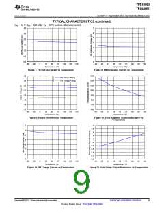
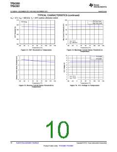
TPS43060
TPS43061
www.ti.com
SLVSBP4A –DECEMBER 2012–REVISED DECEMBER 2012
•
•
•
•
•
VSTOP is the desired turn-off voltage at the VIN pin
VEN_ON is EN pin voltage threshold to enable the device, 1.21V (typical)
VEN_DIS is EN pin voltage threshold to disable the device, 1.14V (typical)
IEN_hys is the hysteresis current inside the device, 3.2μA (typical)
IEN_pup is the internal pull-up current at EN pin, 1.8μA (typical)
VOLTAGE REFERENCE AND SETTING OUTPUT VOLTAGE
An internal voltage reference provides a precise 1.22 V voltage reference at the error amplifier non-inverting
input. To set the output voltage, select the FB pin resistor RSH and RSL according to Equation 4.
æ
ç
è
ö
÷
ø
RSH
RSL
VOUT =1.22V ´
+1
(4)
MINIMUM ON-TIME AND PULSE SKIPPING
The TPS43060 and TPS43061 also feature a minimum on-time of 100 ns for the low-side gate driver. This
minimum on-time determines the minimum duty cycle of the PWM for any set switching frequency. When the
voltage regulation loop requires a minimum on-time pulse width less than 100 ns, the controller enters pulse-
skipping mode. In this mode, the devices hold the power switch off for multiple switching cycles to prevent the
output voltage from rising above the desired regulated voltage. This operation typically occurs in light load
conditions when the DC-DC converter operates in discontinuous conduction mode. Pulse skipping increases the
output ripple as shown in Figure 27.
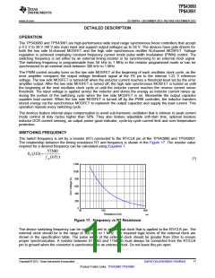
ZERO-CROSS-DETECTION and DUTY CYCLE
The TPS43060 and TPS43061 feature zero-cross-detection which turns off high side driver when the sensed
current falls below the reverse current sense threshold (3.8 mV typical), then the converter runs in discontinuous
conduction mode (DCM). The duty cycle is dependent on the mode in which the converter is operating. The duty
cycle in DCM varies widely with changes of the load. In CCM, where the inductor maintains a minimum dc
current, the duty cycle is related primarily to the input and output voltages as computed in Equation 5.
VOUT -VIN
D =
VOUT
(5)
When the converter operates in DCM, the duty cycle is a function of the load, input and output voltages,
inductance and switching frequency in Equation 6.
2´VOUT ´ IOUT ´ L´ fSW
D =
2
VIN
(6)
Equation 5 and Equation 6 provide an estimation of the duty cycle. A more accurate duty cycle can be calculated
by including the voltage drops of the external MOSFETs, sense resistor and DCR of the inductor.
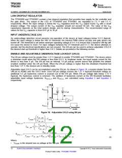
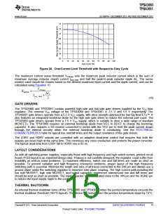
MINIMUM OFF-TIME and MAXIMUM DUTY CYCLE
The low side driver LDRV of TPS43060 and TPS43061 has a minimum off-time of 250 ns or 5% of the switching
cycle period whichever is longer. Figure 19 shows Maximum duty cycle vs. Switching Frequency. The maximum
duty cycle limits the maximum achievable step-up ratio in a Boost converter. When the converter operates in
CCM, the step-up ratio of the boost converter can be calculated using Equation 7.
VOUT
1
=
VIN
1- D
(7)
For instance, if the maximum duty cycle is 90%, the achievable maximum output voltage to input voltage ratio is
limited to:
VOUT
1
=
=10
VIN
1-90%
(8)
13
Copyright © 2012, Texas Instruments Incorporated
Submit Documentation Feedback
Product Folder Links: TPS43060 TPS43061

 TI [ TEXAS INSTRUMENTS ]