TPS43060
TPS43061
www.ti.com
SLVSBP4A –DECEMBER 2012–REVISED DECEMBER 2012
DETAILED DESCRIPTION
OPERATION
The TPS43060 and TPS43061 are high-performance wide input range synchronous boost controllers that accept
a 4.5 V to 38 V (40 V abs max) input and support output voltages up to 58 V. The devices have gate drivers for
both the low side N-channel MOSFET and the high side synchronous rectifier N-channel MOSFET. Voltage
regulation is achieved employing constant frequency current mode pulse width modulation (PWM) control. The
switching frequency is set either by an external timing resistor or by synchronizing to an external clock signal.
The switching frequency is programmable from 50 kHz to 1 MHz in the resistor programmed mode or can be
synchronized to an external clock between 300 kHz to 1 MHz.
The PWM control circuitry turns on the low side MOSFET at the beginning of each oscillator clock cycle, as the
error amplifier compares the output voltage feedback signal at the FB pin to the internal 1.22 V reference
voltage. The low side MOSFET is turned-off when the inductor current reaches a threshold level set by the error
amplifier output. After the low side MOSFET is turned off, the high side synchronous MOSFET is turned on until
the beginning of the next oscillator clock cycle or until the inductor current reaches the reverse current sense
threshold. The input voltage is applied across the inductor and stores the energy as inductor current ramps up
during the portion of the switching cycle when the low side MOSFET is on. Meanwhile the output capacitor
supplies load current. When the low side MOSFET is turned off by the PWM controller, the inductor transfers
stored energy via the synchronous MOSFET to replenish the output capacitor and supply the load current. This
operation repeats every switching cycle.
The devices feature internal slope compensation to avoid sub-harmonic oscillation that is intrinsic to peak current
mode control at duty cycles higher than 50%. They also feature adjustable soft-start time, optional lossless
inductor DCR current sensing, an output power good indicator, cycle-by-cycle current limit and over-temperature
protection.
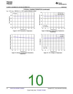
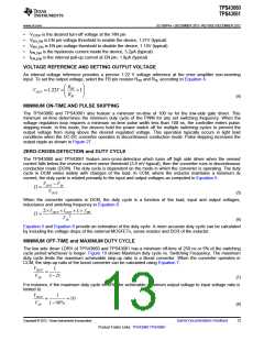
SWITCHING FREQUENCY
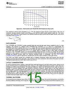
The switch frequency is set by a resistor (RT) connected to the RT/CLK pin of the TPS43060 and TPS43061.
The relationship between the timing resistance RT and frequency is shown in the Figure 17. The resistor value
required for a desired frequency can be calculated using Equation 1.
57500
RT (kW) =
fsw (kHz)
(1)
1200
1000
800
600
400
200
0
30
100
Resistance (kΩ)
900
G001
Figure 17. Frequency vs RT Resistance
The device switching frequency can be synchronized to an external clock that is applied to the RT/CLK pin. The
external clock should be in the range of 300 kHz to 1 MHz. The required logic levels of the external clock are
shown in the specification table. The pulse width of the external clock should be greater than 20ns to ensure
proper synchronization. A resistor between 57.5 kΩ and 1150 kΩ must always be connected from the RT/CLK
pin to ground when the converter is synchronized to an external clock. Do not leave this pin open.
Copyright © 2012, Texas Instruments Incorporated
Submit Documentation Feedback
11
Product Folder Links: TPS43060 TPS43061

 TI [ TEXAS INSTRUMENTS ]