TPS40210-Q1, TPS40211-Q1
www.ti.com
SLVS861D –AUGUST 2008–REVISED APRIL 2010
The load current overcurrent threshold is set by proper choice of RISNS. If the converter is operating in
discontinuous mode the current sense resistor is found in Equation 6.
f
´L ´ V
ISNS(oc)
SW
R
=
ISNS
2´L ´ f
´I
´ V
(
+ V - V
)
SW
OUT(oc)
OUT D IN
(6)
If the converter is operating in continuous conduction mode RISNS can be found in Equation 7.
V
V
ISNS
ISNS
R
=
=
ISNS
I
I
RIPPLE
æ
ç
è
ö
æ
ö
÷
ø
æ
ö
æ
ç
è
ö
÷
ø
I
D´ V
IN
OUT
OUT
+
+
÷
ø
ç
è
ç
ç
÷
÷
1- D
2
1- D
(
2´ f
´L
)
SW
è
ø
where
•
•
•
•
•
•
•
•
RISNS is the value of the current sense resistor in Ω.
VISNS(oc) is the overcurrent threshold voltage at the ISNS pin (from electrical specifications)
D is the duty cycle (from Equation 2)
f SW is the switching frequency in Hz
VIN is the input voltage to the power stage in V (see text)
L is the value of the inductor in H
IOUT(oc) is the desired overcurrent trip point in A
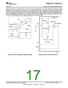
VD is the drop across the diode in Figure 23
(7)
The TPS40210 and TPS40211 have a fixed undervoltage lockout (UVLO) that allows the controller to start at a
typical input voltage of 4.25 V. If the input voltage is slowly rising, the converter might have less than its designed
nominal input voltage available when it has reached regulation. As a result, this may decreases the apparent
current-limit load current value and must be taken into consideration when selecting RISNS. The value of VIN used
to calculate RISNS must be the value at which the converter finishes startup. The total converter output current at
startup is the sum of the external load current and the current required to charge the output capacitor(s). See the
Soft Start section of this data sheet for information on calculating the required output capacitor charging current.
The topology of the standard boost converter has no method to limit current from the input to the output in the
event of a short circuit fault on the output of the converter. If protection from this type of event is desired, it is
necessary to use some secondary protection scheme such as a fuse or rely on the current limit of the upstream
power source.
Current Sense and Sub-Harmonic Instability
A characteristic of peak current-mode control results in a condition where the current control loop can exhibit
instability. This results in alternating long and short pulses from the pulse-width modulator. The voltage loop
maintains regulation and does not oscillate, but the output ripple voltage increases. The condition occurs only
when the converter is operating in continuous conduction mode, and the duty cycle is 50% or greater. The cause
of this condition is described in Texas Instruments literature number SLUA101, available at www.ti.com. The
remedy for this condition is to apply a compensating ramp from the oscillator to the signal going to the
pulse-width modulator. In the TPS40210 and TPS40211, the oscillator ramp is applied in a fixed amount to the
pulse-width modulator. The slope of the ramp is given in Equation 8.
V
æ
ö
VDD
s
= f
´
e
SW
ç
÷
20
è
ø
(8)
To ensure that the converter does not enter into sub-harmonic instability, the slope of the compensating ramp
signal must be at least half of the down slope of the current ramp signal. Because the compensating ramp is
fixed in the TPS40210 and TPS40211, this places a constraint on the selection of the current sense resistor.
The down slope of the current sense wave form at the pulse-width modulator is described in Equation 9.
ACS ´RISNS ´ V
(
+ VD - V
IN
)
OUT
m2 =
L
(9)
15
Copyright © 2008–2010, Texas Instruments Incorporated
Submit Documentation Feedback
Product Folder Link(s): TPS40210-Q1 TPS40211-Q1

 TI [ TEXAS INSTRUMENTS ]