TPS40210-Q1, TPS40211-Q1
www.ti.com
SLVS861D –AUGUST 2008–REVISED APRIL 2010
Setting the Oscillator Frequency
The oscillator frequency is determined by a resistor and capacitor connected to the RC pin of the TPS40210. The
capacitor is charged to a level of approximately VVDD/20 by current flowing through the resistor and is then
discharged by a transistor internal to the TPS40210. The required resistor for a given oscillator frequency is
found from either Figure 1 or Equation 5.
1
R
=
T
-8
5.8 ´10 ´ f
-10
2
-7
-4
-6
- 1.5 ´10 + 1.7 ´10 ´ C - 4 ´10 ´ C
SW T T
-9
2
´ C +8 ´10
´ f
+ 1.4 ´10 ´ f
SW
T
SW
where
•
•
•
RT is the timing resistance in kΩ
f SW is the switching frequency in kHz
CT is the timing capacitance in pF
(5)
For most applications, a capacitor in the range of 68 pF to 120 pF gives the best results. Resistor values should
be limited to between 100 kΩ and 1 MΩ as well. If the resistor value falls below 100 kΩ, decrease the capacitor
size and recalculate the resistor value for the desired frequency. As the capacitor size decreases below 47 pF,
the accuracy of Equation 5 degrades, and empirical means may be needed to fine tune the timing component
values to achieve the desired switching frequency.
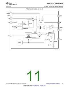
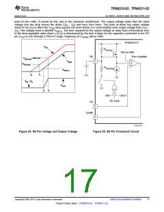
Synchronizing the Oscillator
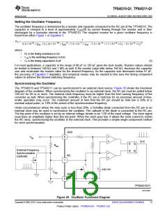
The TPS40210 and TPS40211 can be synchronized to an external clock source. Figure 20 shows the functional
diagram of the oscillator. When synchronizing the oscillator to an external clock, the RC pin must be pulled below
150 mV for 20 ns or more. The external clock frequency must be higher than the free running frequency of the
converter as well. When synchronizing the controller, if the RC pin is held low for an excessive amount of time,
erratic operation may occur. The maximum amount of time that the RC pin should be held low is 50% of a
nominal output pulse, or 10% of the period of the synchronization frequency.
Under circumstances where the duty cycle is less than 50%, a Schottky diode connected from the RC pin to an
external clock may be used to synchronize the oscillator. The cathode of the diode is connected to the RC pin.
The trip point of the oscillator is set by an internal voltage divider to be 1/20 of the input voltage. The clock signal
must have an amplitude higher than this trip point. When the clock goes low, it allows the reset current to restart
the RC ramp, synchronizing the oscillator to the external clock. This provides a simple single-component method
for clock synchronization.
VDD
8
V
IN
CLK
+
S
R
Q
Q
R
RC
External Frequency
Synchronization
(optional)
RC
+
1
5
+
150 mV
C
RC
GND
TPS40210/11
UDG-08063
Figure 20. Oscillator Functional Diagram
Copyright © 2008–2010, Texas Instruments Incorporated
Submit Documentation Feedback
13
Product Folder Link(s): TPS40210-Q1 TPS40211-Q1

 TI [ TEXAS INSTRUMENTS ]