TPS40210-Q1, TPS40211-Q1
SLVS861D –AUGUST 2008–REVISED APRIL 2010
www.ti.com
APPLICATION INFORMATION
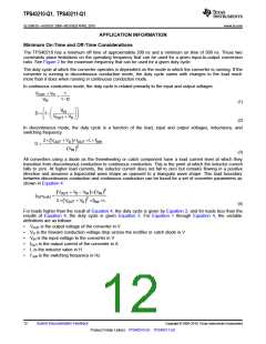
Minimum On-Time and Off-Time Considerations
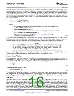
The TPS40210 has a minimum off time of approximately 200 ns and a minimum on time of 300 ns. These two
constraints place limitations on the operating frequency that can be used for a given input-to-output conversion
ratio. See Figure 2 for the maximum frequency that can be used for a given duty cycle.
The duty cycle at which the converter operates is dependent on the mode in which the converter is running. If the
converter is running in discontinuous conduction mode, the duty cycle varies with changes to the load much
more than it does when running in continuous conduction mode.
In continuous conduction mode, the duty cycle is related primarily to the input and output voltages.
VOUT + VD
1
=
V
1- D
IN
(1)
(2)
æ
ö
÷
÷
ø
æ
ç
è
ö
÷
ø
V
IN
D = 1-
ç
ç
è
VOUT + VD
In discontinuous mode, the duty cycle is a function of the load, input and output voltages, inductance, and
switching frequency.
2´ V
(
+ V ´I
)
´L ´ f
OUT
D
OUT SW
D =
2
V
( )
IN
(3)
All converters using a diode as the freewheeling or catch component have a load current level at which they
transition from discontinuous conduction to continuous conduction. This is the point at which the inductor current
falls to zero. At higher load currents, the inductor current does not fall to zero but remains flowing in a positive
direction and assumes a trapezoidal wave shape as opposed to a triangular wave shape. This load boundary
between discontinuous conduction and continuous conduction can be found for a set of converter parameters as
shown in Equation 4.
2
V
(
+ VD - V ´ V
IN ) ( )
IN
OUT
IOUT(crit)
=
2´ V
(
+ VD 2 ´ fSW ´L
)
OUT
(4)
For loads higher than the result of Equation 4, the duty cycle is given by Equation 2, and for loads less than the
results of Equation 4, the duty cycle is given Equation 3. For Equation 1 through Equation 4, the variable
definitions are as follows:
•
•
•
•
•
•
VOUT is the output voltage of the converter in V
VD is the forward conduction voltage drop across the rectifier or catch diode in V
VIN is the input voltage to the converter in V
IOUT is the output current of the converter in A
L is the inductor value in H
f SW is the switching frequency in Hz
12
Submit Documentation Feedback
Copyright © 2008–2010, Texas Instruments Incorporated
Product Folder Link(s): TPS40210-Q1 TPS40211-Q1

 TI [ TEXAS INSTRUMENTS ]