ꢀ
ꢁꢂ
ꢃ
ꢄꢄ
ꢅ
ꢆꢇ
www.ti.com
SLOS407D − FEBRUARY 2003 − REVISED AUGUST 2004
13 mils diameter) should be equally spaced underneath the thermal land. The vias should connect to a
solid copper plane, either on an internal layer or on the bottom layer of the PCB. The vias must be solid
vias, not thermal relief or webbed vias. For additional information, please refer to the PowerPAD Thermally
Enhanced Package application note, TI (SLMA002).
For an example layout, refer to the TPA3004D2 Evaluation Module (TPA3004D2EVM) User Manual, TI
(SLOU158). Both the EVM user manual and the PowerPAD application note are available on the TI web site
at http://www.ti.com.
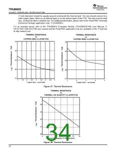
THERMAL RESISTANCE
vs
THERMAL RESISTANCE
vs
COPPER AREA 2-LAYER PCB
COPPER AREA 4-LAYER PCB
35
30
35
30
25
25
20
15
20
15
1
1.5
2
2.5
3
3.5
4
4.5
5
1
2
3
4
5
Copper Area − sq. Inches
Copper Area − sq. Inches
Figure 47. Thermal Resistance
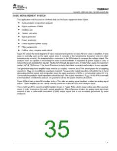
THERMAL RESISTANCE
vs
THERMAL VIA QUANTITY 2-LAYER PCB
25
24
23
22
21
20
4
6
8
10
12
14
16
Thermal Via Quantity (13 Mil Diameter)
Figure 48. Thermal Resistance
34

 TI [ TEXAS INSTRUMENTS ]