www.ti.com
ꢀ ꢁꢂ ꢃꢄꢄ ꢅꢆ ꢇ
SLOS407D − FEBRUARY 2003 − REVISED AUGUST 2004
P
= P
x ((1 / Efficiency) – 1)
O(average)
Dissipated
Efficiency = ~85% for an 8-Ω load
= ~75% for a 4-Ω load
(9)
Example. What is the maximum ambient temperature for an application that requires the TPA3004D2 to drive
10 W into an 8-Ω speaker (stereo)?
P
= 20 W x ((1 / 0.85) – 1) = 3.5 W
(P = 10 W * 2)
O
Dissipated
T
= 125°C – (19°C/W x 3.5 W) = 58.5°C
Amax
This calculation shows that the TPA3004D2 can drive 10 W of continuous RMS power per channel into an 8-Ω
speaker up an ambient temperature of 58.5°C.
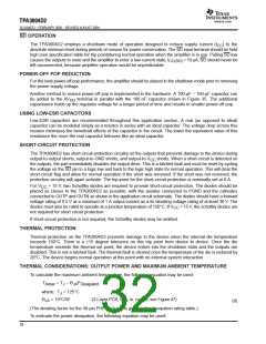
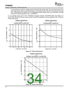
Figure 47 and Figure 48 show the results of several thermal experiments conducted with the TPA3004D2. Both
figures show that the best thermal performance can be achieved with more copper area for heat dissipation
and an adequate number of thermal vias.
Figure 47 shows two curves for a 2-layer and 4-layer PCB. The 2-layer PCB layout was tightly controlled with
a fixed amount of 2 oz. copper on the bottom layer of the PCB. The amount of copper is shown on the x-axis.
Nine thermal vias of 13 mil (0.33 mm) diameter were drilled under the PowerPad and connected to the bottom
layer. The top layer only consisted of traces for signal routing.
The 4-layer PCB layout was also tightly controlled with a fixed amount of 2 oz. copper in middle GND layer. The
top layer only consisted of traces for signal routing. The bottom and other middle layer were left blank. Nine
thermal vias of 0.33mm diameter were drilled under the PowerPAD and connected to the middle layer.
Figure 48 shows the effect of the number of thermal vias drilled under the PowerPad on the thermal
performance of the PCB. The experiment was conducted with a 2-layer PCB and 3 square inches of copper
on the bottom layer. For the best thermal performance, at least 16 vias in a 4x4 pattern should be used under
the PowerPAD. Refer to the TPA3004D2 EVM User’s Manual, SLOU115, for an example layout with a 4x4 via
pattern. PCB gerber files are available at request.
PRINTED CIRCUIT BOARD (PCB) LAYOUT
Because the TPA3004D2 is a class-D amplifier that switches at a high frequency, the layout of the printed circuit
board (PCB) should be optimized according to the following guidelines for the best possible performance.
D
Decoupling capacitors—As described on page 31, the high-frequency 0.1-uF decoupling capacitors
should be placed as close to the PVCC (pin 14, 15, 22, 23, 38, 39, 46, 47) and AV (pin 33) terminals
CC
as possible. The V2P5 (pin 4) capacitor, AV
(pin 29) capacitor, and VCLAMP (pins 25, 36) capacitor
DD
should also be placed as close to the device as possible. Large (10 uF or greater) bulk power supply
decoupling capacitors should be placed near the TPA3004D2 on the PVCCL, PVCCR, and AV
terminals.
CC
D
Grounding—The AV
(pin 33) decoupling capacitor, AV
(pin 29) capacitor, V2P5 (pin 4) capacitor,
DD
CC
COSC (pin 28) capacitor, and ROSC (pin 27) resistor should each be grounded to analog ground (AGND,
pin 26 and pin 30). The PVCC (pin 9 and pin 16) decoupling capacitors should each be grounded to power
ground (PGND, pins 18, 19, 42, 43). Analog ground and power ground may be connected at the
PowerPAD, which should be used as a central ground connection or star ground for the TPA3004D2.
Basically, an island should be created with a single connection to PGND at the PowerPAD.
D
D
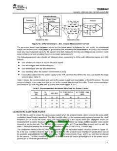
Output filter—The ferrite EMI filter (Figure 41) should be placed as close to the output terminals as
possible for the best EMI performance. The LC filter (Figure 40 should be placed close to the outputs. The
capacitors used in both the ferrite and LC filters should be grounded to power ground.
PowerPAD—The PowerPAD must be soldered to the PCB for proper thermal performance and optimal
reliability. The dimensions of the PowerPAD thermal land should be 5 mm by 5 mm (197 mils by 197 mils).
The PowerPAD size measures 4.55 x 4.55 mm. Four rows of solid vias (four vias per row, 0.3302 mm or
33

 TI [ TEXAS INSTRUMENTS ]