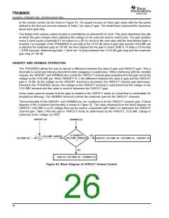
ꢀ
ꢁꢂ
ꢃ
ꢄꢄ
ꢅ
ꢆꢇ
www.ti.com
SLOS407D − FEBRUARY 2003 − REVISED AUGUST 2004
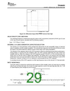
INPUT CAPACITOR, C
I
In the typical application an input capacitor (C ) is required to allow the amplifier to bias the input signal to the
i
proper dc level (V2P5)for optimum operation. In this case, C and the input impedance of the amplifier (Z ) form
i
i
a high-pass filter with the corner frequency determined in equation 6.
−3 dB
(6)
1
f
+
c
2pZ C
i
i
f
c
The value of C is important, as it directly affects the bass (low frequency) performance of the circuit. Consider
i
the example where Z is 20 kΩ and the specification calls for a flat bass response down to 20 Hz. Equation 6
i
is reconfigured as equation 7.
1
C +
i
2pZ f
c
(7)
i
In this example, C is 0.4 µF, so one would likely choose a value in the range of 0.47 µF to 1 µF. If the gain is
i
known and will be constant, use Z from Figure 7 (Input Impedance vs Gain) to calculate C . Calculations for
i
i
C should be based off the impedance at the lowest gain step intended for use in the system. A further
i
consideration for this capacitor is the leakage path from the input source through the input network (C ) and the
i
feedback network to the load. This leakage current creates a dc offset voltage at the input to the amplifier that
reduces useful headroom, especially in high gain applications. For this reason a low-leakage tantalum or
ceramic capacitor is the best choice. When polarized capacitors are used, the positive side of the capacitor
should face the amplifier input in most applications as the dc level there is held at 2.5 V, which is likely higher
than the source dc level. Note that it is important to confirm the capacitor polarity in the application.
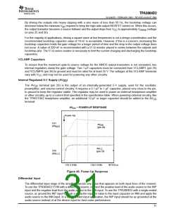
Power Supply Decoupling, C
S
The TPA3004D2 is a high-performance CMOS audio amplifier that requires adequate power supply decoupling
to ensure the output total harmonic distortion (THD) is as low as possible. Power supply decoupling also
prevents oscillations for long lead lengths between the amplifier and the speaker. The optimum decoupling is
achieved by using two capacitors of different types that target different types of noise on the power supply leads.
For higher frequency transients, spikes, or digital hash on the line, a good low equivalent-series-resistance
(ESR) ceramic capacitor, typically 0.1 µF placed as close as possible to the device V
lead works best. For
CC
filtering lower-frequency noise signals, a larger aluminum electrolytic capacitor of 10 µF or greater placed near
the audio power amplifier is recommended. The 10-µF capacitor also serves as local storage capacitor for
supplying current during large signal transients on the amplifier outputs.
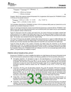
BSN and BSP Capacitors
The full H-bridge output stages use only NMOS transistors. They therefore require bootstrap capacitors for the
high side of each output to turn on correctly. A 10-nF ceramic capacitor, rated for at least 25 V, must be
connected from each output to its corresponding bootstrap input. Specifically, one 10-nF capacitor must be
connected from xOUTP to xBSP, and one 10-nF capacitor must be connected from xOUTN to xBSN. (See the
application circuit diagram in Figure 35.)
The bootstrap capacitors connected between the BSxx pins and corresponding output function as a floating
power supply for the high-side N-channel power MOSFET gate drive circuitry. During each high-side switching
cycle, the bootstrap capacitors attempt to hold the gate-to-source voltage high enough to keep the high-side
MOSFETs turned on. However, there is a leakage path and the voltage on the bootstrap capacitors slowly
decrease while the high-side is conducting.
30

 TI [ TEXAS INSTRUMENTS ]