www.ti.com
Advisory — XINTF Rogue Write for Back-to-Back Accesses to x16/x32 Zones
Advisory
XINTF Rogue Write for Back-to-Back Accesses to x16/x32 Zones
Revision(s) Affected
Details
0
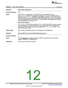
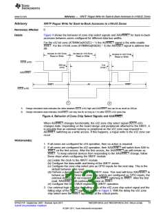
Figure 4 shows the behavior of zone chip select signals and XA0/XWE1 for back-to-back
accesses between zones configured for different data bus widths.
For the x32-bit zone (XTIMINGx[XSIZE] = 1) the A0/XWE1 signal is the write enable
XWE1. For the x16-bit zone (XTIMINGx[XSIZE] = 3) the A0/XWE1 signal is address line
A0.
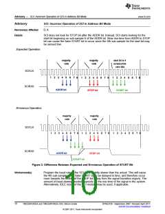
Access to x32 Zone
Read or Write
Access to x16 Zone
Read or Write
Access to x32 Zone
Read or Write
XZCS (x32)
XA0/XWE1
200 ps
(min)
1ns
(max)
A0
XWE1
XWE1
XZCS (x16)
A
B
A
B
Design simulation data indicates the delta between XZCS (x32) high and XA0/XWE1 low can be as small as 200 ps.
Design simulation data indicates XA0/XWE1 can stay low for as long as 1 ns after XZCS (x32) goes low.
Figure 4. Behavior of Zone Chip Select Signals and XA0/XWE1
When A0/XWE1 changes functionality, the x32 zone chip select signal (XZCS x32)
changes state. Depending on the board design and peripherals attached to the XINTF, it
is possible that an external memory or peripheral on the x32 zone may respond to
A0/XWE1 switching as a write access. If this happens, a rogue write to the x32 zone can
occur.
Workaround(s)
1. If all zones are configured for x16 operation, then no action is required.
2. If all zones are configured for x32 operation, then XA0/XWE1 will switch from XA0 to
XWE1 on the first access. After the first access, the XA0/XWE1 pin will remain as
XWE1. To keep external devices from responding to the XA0/XWE1 change, follow
these steps when configuring the XINTF module:
(a) Enable the clock to the XINTF module.
(b) Configure the data-width and timing of the XINTF zones.
(c) Configure the zone chip select pins as GPIO inputs for the next step. This is the
default behavior after reset.
(d) Perform a dummy read from a x32 XINTF zone. This read will force XA0/XWE1 to
behave as XWE1. Since the zone chip selects are configured as GPIO inputs, the
external devices will not respond to XA0/XWE1 switching to XWE1. After the first
read, XA0/XWE1 will continue to behave as XWE1.
(e) Configure the GPIO MUX registers for XINTF operation.
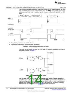
3. Use external logic to delay the falling edge of the x32 zone chip select signal and the
falling edge of the XWE1 signal as shown in Figure 5. With the delay the x32 zone
chip select sees the XWE1 signal high at the critical points.
13
SPRZ272F–September 2007–Revised April 2011
TMS320F2833x and TMS320F2823x DSC Silicon Errata
Submit Documentation Feedback
© 2007–2011, Texas Instruments Incorporated

 TI [ TEXAS INSTRUMENTS ]