Advisory — XINTF Rogue Write for Back-to-Back Accesses to x16/x32 Zones
www.ti.com
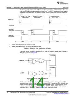
The timing configuration of the x32 zone must account for the additional delay. The zone
chip select delay may require additional lead time. The XWE1 delay enable may require
additional active write time. In addition, specify at least 1 trail cycle for writes to the x32
zone.
Access to x32 Zone
Read or Write
Access to x16 Zone
Read or Write
Access to x32 Zone
Read or Write
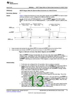
XZCS (x32)
XZCS (x16)
A
A
XA0/XWE1
for x32 zone
B
B
B
XA0/XWE1
for x16 zone
XWE1
A0
XWE1
A
B
Delayed falling edge of zone chip select for x32 zone.
Delayed falling edge of XWE1. The x16 zone will not see this delay.
Figure 5. Behavior After Application of Delay
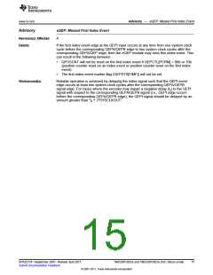
The delay can be created by using 74LVC32 quad OR gates or similar logic to create a
delay line as shown in Figure 6.
Low 16 Bits
XZCS (x32)
CE
High 16 Bits
CE
A0/XWE1
WE
XWE1
Figure 6. Example Delay Line Circuit
This has been fixed in Rev A silicon. The external delay logic is no longer required to
avoid this issue in Rev A. The behavior of the XA0/XWE1 signal has been modified such
that it goes high during inactive cycles. Use the XBANK feature to force inactive cycles
between back-to-back zone accesses. See the TMS320x2833x, 2823x DSC External
Interface (XINTF) Reference Guide (SPRU949) for more information.
14
TMS320F2833x and TMS320F2823x DSC Silicon Errata
SPRZ272F–September 2007–Revised April 2011
Submit Documentation Feedback
© 2007–2011, Texas Instruments Incorporated

 TI [ TEXAS INSTRUMENTS ]