TMS320TCI6487
TMS320TCI6488
Communications Infrastructure Digital Signal Processor
SPRS358F–APRIL 2007–REVISED AUGUST 2008
www.ti.com
3 Device Configuration
On the TCI6487/8 device, certain device configurations (like boot mode, pin multiplexing, and endianness)
are selected at device reset. The status of the peripherals (enabled/disabled) is determined after device
reset. By default, the peripherals on the device are disabled and must be enabled by software before
being used.
3.1 Device Configuration at Device Reset
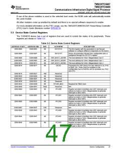
Table 3-1 describes the TCI6487/8 device configuration pins. The logic level is latched at reset to
determine the device configuration. The logic level on the device configuration pins can be set by using
external pullup/pulldown resistors or by using some control device to intelligently drive these pins. When
using a control device, take care to avoid contention on the lines when the device is out of reset. The
device configuration pins are sampled during power-on reset and are driven after the reset is removed. To
avoid contention, the control device must stop driving the device configuration pins of the DSP.
NOTE
If a configuration pin must be routed out from the device, the internal pullup/pulldown
(IPU/IPD) resistor should not be relied upon; TI recommends the use of an external
pullup/pulldown resistor.
Table 3-1. Device Configuration Pins
CONFIGURATION
DEFAULT IPU/IPD
FUNCTIONAL DESCRIPTION
PIN
BOOTMODE[3:0]
LENDIAN
0000b
1b
Boot Mode Selection
Device Endian Mode
0
1
Big Endian
Little Endian
DEVNUM[3:0]
L2_CONFIG
0000b
0b
Device number
L2 Configuration
0
1
C64x+ Megamodule Core
0 = 1536KB, C64x+ Megamodule Core
1 = 1024KB, C64x+ Megamodule Core
2 = 512KB
C64x+ Megamodule Core
0 = 1024KB, C64x+ Megamodule Core
1 = 1024KB, C64x+ Megamodule Core
2 = 1024KB
CORECLKSEL
0b
Core Clock Select
0
1
SYSCLK is shared between the Antenna Interface and the input to PLLCTL1.
ALTCORECLK is used as the input to PLLCTL1 and SYSCLK is used only for the
Antenna Interface.
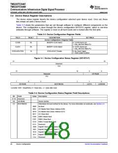
3.2 Peripheral Selection After Device Reset
Several of the peripherals on the TCI6487/8 device are controlled by the Power Sleep Controller (PSC).
By default the AIF, RAC (6488 Only), SRIO, TCP, and VCP are held in reset and clock-gated. The
memories in these modules are also in a low-leakage sleep mode. Software will be required to turn these
memories on then enable the modules (turn on clocks and de-assert reset) before these modules can be
used.
Additionally, the C64x+ Core 0 RSAs, C64x+ Core 1 RSAs, and C64x+ Core 2 RSAs come up clock-gated
and held in reset. Memories in these accelerators are enabled already unlike the previous modules.
Software will be required to enable these modules before they are used as well.
46
Device Configuration
Submit Documentation Feedback

 TI [ TEXAS INSTRUMENTS ]