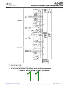
TMS320TCI6487
TMS320TCI6488
Communications Infrastructure Digital Signal Processor
www.ti.com
SPRS358F–APRIL 2007–REVISED AUGUST 2008
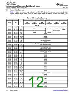
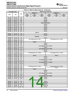
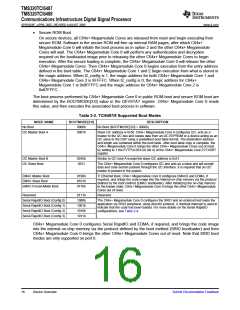
Table 2-2. Memory Map Summary (continued)
HEX ADDRESS RANGE
MEMORY BLOCK DESCRIPTION
SYMMETRIC L2
ASYMMETRIC L2
SIZE
C64x+
MEGAMODULE
CORE 0
C64x+
MEGAMODULE
CORE 1
C64x+
MEGAMODULE
CORE 2
C64x+
MEGAMODULE
CORE 0
C64x+
MEGAMODULE
CORE 1
C64x+
MEGAMODULE
CORE 2
START
END
3C00 0000
3C01 0000
4000 0000
5000 0000
5010 0000
5800 0000
5801 0000
6000 0000
6040 0000
7000 0000
7000 0100
8000 0000
A000 0000
B000 0000
C000 0000
D000 0000
E000 0000
F000 0000
3C00 FFFF
3FFF FFFF
4FFF FFFF
500F FFFF
57FF FFFF
5800 FFFF
5FFF FFFF
603F FFFF
6FFF FFFF
7000 00FF
7FFF FFFF
9FFF FFFF
AFFF FFFF
BFFF FFFF
CFFF FFFF
DFFF FFFF
EFFF FFFF
FFFF FFFF
64K
64M - 64K
256M
1M
L3 ROM
Reserved
Reserved
TCP2 Data
Reserved
127M
64K
VCP2 Data
Reserved
128M 64K
4M
Reserved
252M
256
Reserved
DDR2 EMIF Configuration
Reserved
256M - 256
512M
256M
256m
256m
256m
256m
256m
DDR2 EMIF Data
AIF Data
Reserved
Reserved
Reserved
Reserved
Reserved
2.4 Boot Sequence
The boot sequence is a process by which the DSP's internal memory is loaded with program and data
sections. The DSP's internal registers are programmed with predetermined values. The boot sequence is
started automatically after each power-on reset, warm reset, and system reset. A local reset to an
individual C64x+ Megamodule should not affect the state of the hardware boot controller on the device.
For more details on the initiators of the resets, see Section 8.6, Reset Controller.
The TCI6487/8 supports several boot processes begins execution at the ROM base address, which
contains the bootloader code necessary to support various device boot modes. The boot processes are
software driven; using the BOOTMODE[3:0] device configuration inputs to determine the software
configuration that must be completed.
2.4.1 Boot Modes Supported
The device supports several boot processes, which leverage the internal boot ROM. Most boot processes
are software driven, using the BOOTMODE[3:0] device configuration inputs to determine the software
configuration that must be completed. From a hardware perspective, there are three possible boot modes:
•
No Boot (BOOTMODE[3:0] = 0000b)
With no boot, the CPU executes directly from the internal L2 RAM located at address 0x80 0000.
Note: Device operations are undefined if invalid code is located at address 0x80 0000. This boot mode
is a hardware boot mode.
•
Public ROM Boot
The C64x+ Megamodule Core 0 is released from reset and begins executing from the L3 ROM base
address. C64x+ Megamodule Core 0 is responsible for performing the boot process (e.g., from I2C
ROM, Ethernet, or RapidIO), after which C64x+ Megamodule Core 0 brings the other C64x+
megamodule cores out of reset by setting to 1 the EVTPULSE4 bit (bit 4) of the C64x+ Megamodule
Core 0's EVTASRT register. This process is valid only once: writing 1, then writing 1 again will not
bring Core 1 and 2 out of reset again. Then, the C64x+ Megamodule Core 0 begins execution from the
entry address defined in the boot table. The C64x+ Megamodule Core 1 and 2 begin execution from
their L2 RAMs' base address.
Submit Documentation Feedback
Device Overview
15

 TI [ TEXAS INSTRUMENTS ]