TMS320TCI6487
TMS320TCI6488
Communications Infrastructure Digital Signal Processor
SPRS358F–APRIL 2007–REVISED AUGUST 2008
www.ti.com
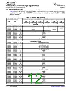
2.3 Memory Map Summary
Table 2-2 shows the memory map address of the TCI6487/8 device. The external memory configuration
register address ranges in the TCI6487/8 device begins at the hex address location 0x7000 for DDR2
Memory Controller.
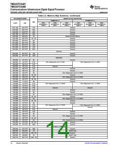
Table 2-2. Memory Map Summary
HEX ADDRESS RANGE
MEMORY BLOCK DESCRIPTION
SYMMETRIC L2
ASYMMETRIC L2
SIZE
C64x+
MEGAMODULE
CORE 0
C64x+
MEGAMODULE
CORE 1
C64x+
MEGAMODULE
CORE 2
C64x+
MEGAMODULE
CORE 0
C64x+
MEGAMODULE
CORE 1
C64x+
MEGAMODULE
CORE 2
START
END
Internal RAM
0000 0000
0080 0000
0088 0000
009 00000
0098 0000
00A0 0000
00E0 0000
00E0 8000
00F0 0000
00F0 8000
0100 0000
01C0 0000
007F FFFF
0087 FFFF
008F FFFF
0097 FFFF
009F FFFF
00DF FFFF
00E0 7FFF
00EF FFFF
00F0 7FFF
00FF FFFF
01BF FFFF
027F FFFF
8M
512K
512K
512K
512K
4M
Reserved
L2 SRAM
L2 SRAM
Reserved
L2 SRAM
Reserved
L2 SRAM
Reserved
Reserved
Reserved
Reserved
32K
L1P SRAM
Reserved
L1D SRAM
Reserved
1M - 32K
32K
1M - 32K
4M
C64x+ Megamodule Registers
Reserved
12.5M
Control Registers on CFG SCR
Frame Synchronization (FSYNC)
0280 0000
0280 0400
0288 0000
0288 0400
0288 0404
0288 0408
0288 040C
0288 0800
0288 0900
0288 0904
0288 0908
0288 090C
0288 0940
0288 0944
0288 0948
0288 0C00
028C 0000
028C 0100
028D 0000
028D 0100
028E 0000
0290 0000
0290 0040
0291 0000
0291 0040
0292 0000
0292 0040
0293 0000
0293 0040
0294 0000
0294 0040
0295 0000
0280 03FF
0287 FFFF
0288 03FF
0288 0403
0288 0407
0288 040B
0288 07FF
0288 0BFF
0288 0903
0288 0907
0288 090B
0288 093F
0288 0943
0288 0947
0288 094B
028B FFFF
028C 00FF
028C FFFF
208D 00FF
028D FFFF
028F FFFF
0290 003F
0290 FFFF
0291 003F
0291 FFFF
0292 003F
0292 FFFF
0293 003F
0293 FFFF
0294 003F
0294 FFFF
0295 003F
1K
511K
1K
Reserved
Chip Interrupt Controller (CIC)
4
DSP Trace Formatter 1 (DTF1)
4
DSP Trace Formatter 2 (DTF2)
DSP Trace Formatter 3 (DTF3)
Reserved
4
1K- 6
1K
CFGC
4B
IPCGR0
4B
IPCGR1
4B
IPCGR2
52B
Reserved
4B
IPCAR0
4B
IPCAR1
4B
IPCAR2
253K
256
Reserved
McBSP0
64K - 256
256
Reserved
McBSP1
64K - 256
128K
64
Reserved
Reserved
Timer Pin Manager (TPMGR)
Reserved
64K - 64
64
Timer0
64K - 64
64
Reserved
Timer1
64K - 64
64
Reserved
Timer2
64K - 64
64
Reserved
Timer3
64K - 64
64
Reserved
Timer4
12
Device Overview
Submit Documentation Feedback

 TI [ TEXAS INSTRUMENTS ]