TMS320TCI6487
TMS320TCI6488
Communications Infrastructure Digital Signal Processor
SPRS358F–APRIL 2007–REVISED AUGUST 2008
www.ti.com
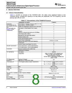
2 Device Overview
2.1 Device Characteristics
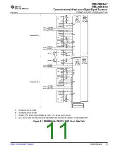
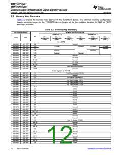
Table 2-1 provides an overview of the TCI6487/8 DSP. The tables show significant features of the
TCI6487/8 device, including the capacity of on-chip RAM, the peripherals, the CPU frequency, and the
package type with pin count.
Table 2-1. Characteristics of the TCI6487/8 Processor
HARDWARE FEATURES
TCI6487/8
Peripherals
DDR2 Memory Controller (32-bit bus width) [1.8 V I/O]
(clock memory = DDRREFCLK(N|P)
1
Not all peripherals pins
are available at the same
time.
(For more detail, see
Section 3, Device
Configuration)
EDMA3 (64 independent channels [CPU/3 clock rate]
High-speed 1x Serial RapidIO Port (2 lanes)
I2C
1
1
1
McBSPs
2
(internal or external clock source up to 100 Mbps)
1000 Ethernet MAC (EMAC)
Management Data Input/Output (MDIO)
Antenna Interface (AIF)
1
1
1
1
Frame Synchronization (FSYNC)
64-bit Timers (Configurable)
(internal clock source CPU/6 clock frequency)
6 64-bit or 12 32-bit
SYSCLKOUT
1
General Purpose Input/Output Port (GPIO)
VCP2 (clock source = CPU/3 clock frequency)
TCP2 (clock source = CPU/3 clock frequency)
Receive Accelerator (RAC) (6488 Only)
Rake/Search Accelerator
16
Decoder Coprocessors
Accelerators
1
1
1
6
On-Chip Memory
Size (Bytes)
3200 KB
Organization
32KB L1P Program Cache (SRAM/Cache)
32KB L1D Data Cache (SRAM/Cache)
32KB Data Memory Controller
3072KB Total L2 Unified Memory SRAM/Cache
64KB L3 ROM
CPU Megamodule
Revision ID
Revision ID Register
(MM_REVID. [15:0]) 0x0181 2000)
0x0
JTAG Device_ID
JTAG Register (address location: 0x0288 0814)
Rev. 1.0 JTAG ID = 0x0009 202Fh (VARIANT =
0000b)
Rev. 1.1 JTAG ID = 0x1009 202Fh (VARIANT =
0001b)
Frequency
Cycle Time
Voltage
MHz
1000 (1.0 GHz)
1-ns [1.0 GHz CPU]
0.9 V to 1.1 V
ns
Core (V)
I/O (V)
1.8 V, 1.1 V
PLL1 and PLL1 Controller CLKIN1 Frequency Multiplier
Options
Bypass (x1), (x4 to x32)
PLL2
DDR Clock
23 X 23 mm
µm
X10
561-Pin Flip-Chip with BGA CUN/GUN/ZUN
0.065 µm
BGA Package
Process Technology
8
Device Overview
Submit Documentation Feedback

 TI [ TEXAS INSTRUMENTS ]