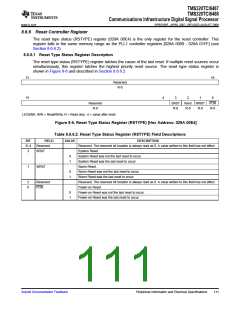
TMS320TCI6487
TMS320TCI6488
Communications Infrastructure Digital Signal Processor
www.ti.com
SPRS358F–APRIL 2007–REVISED AUGUST 2008
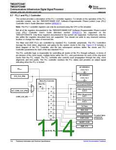
8.7.1 PLL1 Controller Device-Specific Information
8.7.1.1 Internal Clocks and Maximum Operating Frequencies
The Main PLL, used to drive all of the cores, the switch fabric, and a majority of the peripheral clocks (all
but the DDR2 clocks) requires a PLL controller to manage the various clock divisions, gating, and
synchronization. The Main PLL controller has seven CPU/6 outputs that are listed below, along with the
clock description. Each CPU/6 has a corresponding divide that divides down the output clock of the PLL.
Note that dividers are not programmable unless explicitly mentioned in the description below.
•
•
•
•
SYSCLK1 - SYSCLK6: Reserved.
SYSCLK7: Full-rate clock for all C64x+ Megamodules and RSAs.
SYSCLK8: 1/4-rate clock (rac_clk) for the RAC subsystem.
SYSCLK9: 1/3-rate clock (chip_clk3) for the switch fabrics, CIC blocks, and fast peripherals (AIF,
SRIO, TCP, VCP, EDMA).
•
•
SYSCLK10: 1/6-rate clock (chip_clk6) for other peripherals (PLL Controllers, McBSPs, Timer64s,
Semaphore, EMAC, GPIO, I2C, PSC) and L3 ROM.
SYSCLK11: 1/n-rate clock (chip_clks) for an optional McBSP CLKS module input to drive the clock
generator. Default for this will be 1/10. This is programmable from /6 to /32, where this clock does not
violate the max clock of 104.48 MHz. This clock is also output to the SYSCLKOUT pin.
•
•
SYSCLK12: 1/2-rate clock used to clock the L2 and L2 Powerdown Controller.
SYSCLK13: 1/n-rate clock for trace. Default rate for this will be 1/6. This is programmable from /1 to
/32, where this clock does not violate the max of 333 MHz. Please note that the data rate on the trace
pins are 1/2 of this clock.
8.7.1.2 PLL1 Controller Operating Modes
The PLL1 controller has two modes of operation: bypass mode and PLL mode. The mode of operation is
determined by the PLLEN bit of the PLL control register (PLLCTL). In PLL mode, SYSREFCLK is
generated from the device input clock CLKIN1 using the divider PREDIV and the PLL multiplier PLLM. In
bypass mode, CLKIN1 is fed directly to SYSREFCLK.
All hosts must hold off accesses to the DSP while the frequency of its internal clocks is changing. A
mechanism must be in place such that the DSP notifies the host when the PLL configuration has
completed.
8.7.1.3 PLL1 Stabilization, Lock, and Reset Times
The PLL stabilization time is the amount of time that must be allotted for the internal PLL regulators to
become stable after device powerup. The PLL should not be operated until this stabilization time has
expired.
The PLL reset time is the amount of wait time needed when resetting the PLL (writing PLLRST = 1), in
order for the PLL to properly reset, before bringing the PLL out of reset (writing PLLRST = 0). For the
PLL1 reset time value, see Table 8-19.
The PLL lock time is the amount of time needed from when the PLL is taken out of reset (PLLRST = 1
with PLLEN = 0) to when the PLL controller can be switched to PLL mode (PLLEN = 1). The PLL1 lock
time is given in Table 8-20.
Table 8-19. PLL1 Stabilization, Lock, and Reset Times(1)
MIN
TYPE
MAX
UNIT
PLL1 Stabilization Time
PLL Lock Time
100
µS
2000P
PLL Reset Time
1000
ns
(1) P = CLKIN1 cycle time in ns.
Submit Documentation Feedback
Peripheral Information and Electrical Specifications
115

 TI [ TEXAS INSTRUMENTS ]