TMS320TCI6487
TMS320TCI6488
Communications Infrastructure Digital Signal Processor
SPRS358F–APRIL 2007–REVISED AUGUST 2008
www.ti.com
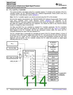
8.7 PLL1 and PLL1 Controller
This section provides a description of the PLL1 controller registers. For details on the operation of the PLL
controller module, see the TMS320TCI6488 DSP Software-Programmable Phase-Locked Loop (PLL)
Controller User's Guide (literature number SPRUEF1).
Note: The PLL1 controller registers can only be accessed using the CPU or the emulator.
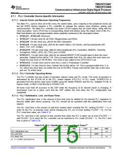
Not all of the registers documented in the TMS320TCI6488 DSP Software-Programmable Phase-Locked
Loop (PLL) Controller User's Guide (literature number SPRUEF1) are supported on the
TMS320TCI6487/8. Only those registers documented in this section are supported. Furthermore, only the
bits within the registers described here are supported. You should not write to any reserved memory
location or change the value of reserved bits.
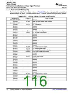
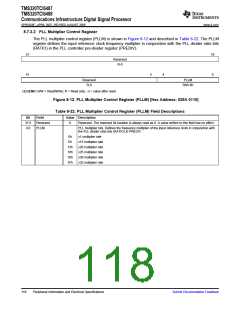
The Main and DDR PLLs are controlled by standard PLL Controller peripherals. The PLL Controllers
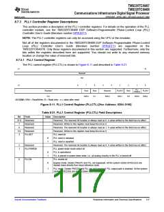
manage the clock ratios, alignment, and gating for the system clocks to the chip. Figure 8-10 includes a
block diagram of the PLL Controller, and the two subsequent sections define the clocks and PLL
Controller parameters for each of the two standard PLLs.
The PLL controller logic is responsible for controlling all modes of the PLL through software, in terms of
pre-division of the clock inputs, multiply factor within the PLL, and post-division for each of the chip-level
clocks from the PLL output. The PLL controller also controls reset propagation through the chip, clock
alignment, and test points. The PLL controller monitors the PLL status and provides an output signal
indicating when the PLL is locked.
AIF SERDES 0
AVDD118
x12.5, 10, 4
AIF SERDES 1
SYS_CLK_(PIN)
x12.5, 10, 4
Main.PLL Controller
Main PLL
To L2 and L2 PDCTL
0
1
xM
/1
.
.
C64x+ Megamodule
Core 0
ALT_CORE_CLK_(PIN)
CORE_CLK_SEL
/2
/n
/4
.
.
C64x+ Megamodule
Core 1
.
.
C64x+ Megamodule
Core 2
.
.
/3
.
.
To Trace
RAC_CLK
/6
.
.
/m
.
.
CHIP_CLK3
CHIP_CLK6
McBSP_CLKS
EMIF_PTV
To switch fabric
peripherals,
/20
/20
.
.
accelerators
Figure 8-10. PLL Controller Diagram
114
Peripheral Information and Electrical Specifications
Submit Documentation Feedback

 TI [ TEXAS INSTRUMENTS ]