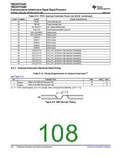
TMS320TCI6487
TMS320TCI6488
Communications Infrastructure Digital Signal Processor
SPRS358F–APRIL 2007–REVISED AUGUST 2008
www.ti.com
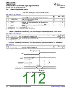
8.6.7 Reset Electrical Data/Timing
Table 8-16. Timing Requirements for Reset(1)(2)
(see Figure 8-7 and Figure 8-8)
NO.
MIN
100
100
24C
12C
MAX UNIT
1
2
4
7
th(SUPPLY-POR)
tsu(XWRSTH-PORH)
tw(XWRST)
Hold Time, POR low after supplies stable and input clocks valid
Setup Time, XWRSTx high to POR high
Pulse Duration, XWRST low
µs
µs
ns
ns
ts(BOOT)
Setup time, boot mode and configuration pins valid before POR
or XWRST high
8
th(BOOT)
Hold time, bootmode and configuration pins valid after POR or
XWRST high
12C
ns
(1) If CORECLKSEL = 0, C = 1/SYSCLK(N|P) frequency, in ns.
(2) If CORECLKSEL = 1, C = 1/ALTCORECLK(N|P) frequency, in ns.
Table 8-17. Switching Characteristics Over Recommended Operating Conditions During Reset(1)
(see Figure 8-7 and Figure 8-8)
NO.
3
MIN
MAX UNIT
td(PORH-RSTATH)
Delay Time, POR high to RESETSTAT high
21000C
35C
ns
ns
5
td(XWRSTH-RSTATH) Delay Time, XWRST high to RESETSTAT high
(1) C = 1/CPU frequency, in ns.
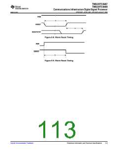
Table 8-18. Switching Characteristics Over Recommended Operating Conditions for Warm Reset
(see Figure 8-9)
NO.
MIN
MAX UNIT
9
tsu(PORH-XWRSTL)
Setup time, POR high to XWRST low
1.34
ms
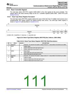
1
2
POR
XWRST
3
RESETSTAT
7
Boot and Device
Configuration Pins
8
Figure 8-7. Power-On Reset Timing
112
Peripheral Information and Electrical Specifications
Submit Documentation Feedback

 TI [ TEXAS INSTRUMENTS ]