TMS320DM6437
Digital Media Processor
www.ti.com
SPRS345B–NOVEMBER 2006–REVISED MARCH 2007
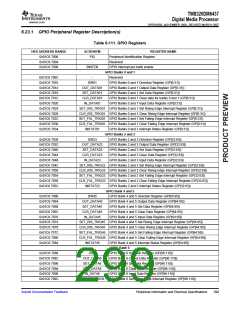
6.23.1 GPIO Peripheral Register Description(s)
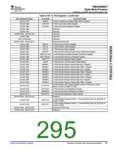
Table 6-111. GPIO Registers
HEX ADDRESS RANGE
0x01C6 7000
ACRONYM
REGISTER NAME
PID
-
Peripheral Identification Register
Reserved
0x01C6 7004
0x01C6 7008
BINTEN
GPIO interrupt per-bank enable
GPIO Banks 0 and 1
0x01C6 700C
0x01C6 7010
0x01C6 7014
0x01C6 7018
0x01C6 701C
0x01C6 7020
0x01C6 7024
0x01C6 7028
0x01C6 702C
0x01C6 7030
0x01C6 7034
-
Reserved
DIR01
GPIO Banks 0 and 1 Direction Register (GP[0:31])
GPIO Banks 0 and 1 Output Data Register (GP[0:31])
GPIO Banks 0 and 1 Set Data Register (GP[0:31])
GPIO Banks 0 and 1 Clear data for banks 0 and 1 (GP[0:31])
GPIO Banks 0 and 1 Input Data Register (GP[0:31])
OUT_DATA01
SET_DATA01
CLR_DATA01
IN_DATA01
SET_RIS_TRIG01 GPIO Banks 0 and 1 Set Rising Edge Interrupt Register (GP[0:31])
CLR_RIS_TRIG01 GPIO Banks 0 and 1 Clear Rising Edge Interrupt Register (GP[0:31])
SET_FAL_TRIG01 GPIO Banks 0 and 1 Set Falling Edge Interrupt Register (GP[0:31])
CLR_FAL_TRIG01 GPIO Banks 0 and 1 Clear Falling Edge Interrupt Register (GP[0:31])
INSTAT01
GPIO Banks 0 and 1 Interrupt Status Register (GP[0:31])
GPIO Banks 2 and 3
0x01C6 7038
0x01C6 703C
0x01C6 7040
0x01C6 7044
0x01C6 7048
0x01C6 704C
0x01C6 7050
0x01C6 7054
0x01C6 7058
0x01C6 705C
DIR23
GPIO Banks 2 and 3 Direction Register (GP[32:63])
GPIO Banks 2 and 3 Output Data Register (GP[32:63])
GPIO Banks 2 and 3 Set Data Register (GP[32:63])
GPIO Banks 2 and 3 Clear Data Register (GP[32:63])
GPIO Banks 2 and 3 Input Data Register (GP[32:63])
OUT_DATA23
SET_DATA23
CLR_DATA23
IN_DATA23
SET_RIS_TRIG23 GPIO Banks 2 and 3 Set Rising Edge Interrupt Register (GP[32:63])
CLR_RIS_TRIG23 GPIO Banks 2 and 3 Clear Rising Edge Interrupt Register (GP[32:63])
SET_FAL_TRIG23 GPIO Banks 2 and 3 Set Falling Edge Interrupt Register (GP[32:63])
CLR_FAL_TRIG23 GPIO Banks 2 and 3 Clear Falling Edge Interrupt Register (GP[32:63])
INSTAT23
GPIO Banks 2 and 3 Interrupt Status Register (GP[32:63])
GPIO Bank 4 and 5
0x01C6 7060
0x01C6 7064
0x01C6 7068
0x01C6 706C
0x01C6 7070
0x01C6 7074
0x01C6 7078
0x01C6 707C
0x01C6 7080
0x01C6 7084
DIR45
GPIO Bank 4 and 5 Direction Register (GP[64:95])
GPIO Bank 4 and 5 Output Data Register (GP[64:95])
GPIO Bank 4 and 5 Set Data Register (GP[64:95])
GPIO Bank 4 and 5 Clear Data Register (GP[64:95])
GPIO Bank 4 and 5 Input Data Register (GP[64:95])
OUT_DATA45
SET_DATA45
CLR_DATA45
IN_DATA45
SET_RIS_TRIG45 GPIO Bank 4 and 5 Set Rising Edge Interrupt Register (GP[64:95])
CLR_RIS_TRIG45 GPIO Bank 4 and 5 Clear Rising Edge Interrupt Register (GP[64:95])
SET_FAL_TRIG45 GPIO Bank 4 and 5 Set Falling Edge Interrupt Register (GP[64:95])
CLR_FAL_TRIG45 GPIO Bank 4 and 5 Clear Falling Edge Interrupt Register (GP[64:95])
INSTAT45
GPIO Bank 4 and 5 Interrupt Status Register (GP[64:95])
GPIO Bank 6
0x01C6 7088
0x01C6 708C
0x01C6 7090
0x01C6 7094
0x01C6 7098
0x01C6 709C
DIR6
GPIO Bank 6 Direction Register (GP[96:110])
GPIO Bank 6 Output Data Register (GP[96:110])
GPIO Bank 6 Set Data Register (GP[96:110])
GPIO Bank 6 Clear Data Register (GP[96:110])
GPIO Bank 6 Input Data Register (GP[96:110])
GPIO Bank 6 Set Rising Edge Interrupt Register (GP[96:110])
OUT_DATA6
SET_DATA6
CLR_DATA6
IN_DATA6
SET_RIS_TRIG6
Submit Documentation Feedback
Peripheral Information and Electrical Specifications
299

 TI [ TEXAS INSTRUMENTS ]