TMS320DM6437
Digital Media Processor
www.ti.com
SPRS345B–NOVEMBER 2006–REVISED MARCH 2007
6.23 General-Purpose Input/Output (GPIO)
The GPIO peripheral provides general-purpose pins that can be configured as either inputs or outputs.
When configured as an output, a write to an internal register can control the state driven on the output pin.
When configured as an input, the state of the input is detectable by reading the state of an internal
register. In addition, the GPIO peripheral can produce CPU interrupts and EDMA events in different
interrupt/event generation modes. The GPIO peripheral provides generic connections to external devices.
The GPIO pins are grouped into banks of 16 pins per bank (i.e., bank 0 consists of GP[0:15]).
The DM6437 GPIO peripheral supports the following:
•
•
Up to 111 3.3-V GPIO pins, GP[0:110]
Interrupts:
–
–
–
Up to 8 unique GP[0:7] interrupts from Bank 0
7 GPIO bank (aggregated) interrupt signals from each of the 7 banks of GPIOs
Interrupts can be triggered by rising and/or falling edge, specified for each interrupt capable GPIO
signal
•
•
DMA events:
–
–
Up to 8 unique GPIO DMA events from Bank 0
7 GPIO bank (aggregated) DMA event signals from each of the 7 banks of GPIOs
Set/clear functionality: Firmware writes 1 to corresponding bit position(s) to set or to clear GPIO
signal(s). This allows multiple firmware processes to toggle GPIO output signals without critical section
protection (disable interrupts, program GPIO, re-enable interrupts, to prevent context switching to
anther process during GPIO programming).
•
•
Separate Input/Output registers
Output register in addition to set/clear so that, if preferred by firmware, some GPIO output signals can
be toggled by direct write to the output register(s).
•
Output register, when read, reflects output drive status. This, in addition to the input register reflecting
pin status and open-drain I/O cell, allows wired logic be implemented.
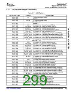
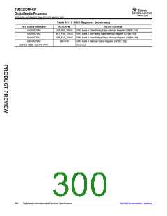
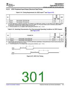
The memory map for the GPIO registers is shown in Table 6-111. For more detailed information on
GPIOs, see the TMS320DM643x DMP General-Purpose Input/Output (GPIO) User's Guide (literature
number SPRU988).
298
Peripheral Information and Electrical Specifications
Submit Documentation Feedback

 TI [ TEXAS INSTRUMENTS ]