TMS320DM6437
Digital Media Processor
www.ti.com
SPRS345B–NOVEMBER 2006–REVISED MARCH 2007
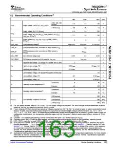
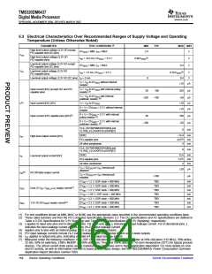
5.2 Recommended Operating Conditions(1)
MIN
1.14
NOM
1.2
MAX
1.26
UNIT
V
(-600, -500, -400
devices)
(2)
CVDD
Supply voltage, Core (CVDD, VDDA_1P1V)
(-400 devices)
1.0
1.05
3.3
1.1
V
V
Supply voltage, I/O, 3.3V (DVDD33
)
3.14
3.46
DVDD
Supply voltage, I/O, 1.8V (DVDDR2, DDR_VDDDLL, PLLPWR18
,
1.71
1.8
0
1.89
V
V
(3)
VDDA_1P8V, MXVDD
)
Supply ground (VSS, VSSA_1P8V, VSSA_1P1V, DDR_VSSDLL,
VSS
0
0
(4)
MXVSS
)
DDR_VREF
DDR_ZP
DDR2 reference voltage(5)
0.49DVDDR2
0.5DVDDR2
VSS
0.51DVDDR2
V
V
DDR2 impedance control, connected via 200 Ω resistor to VSS
DDR2 impedance control, connected via 200 Ω resistor to
DVDDR2
DDR_ZN
DVDDR2
V
DAC_VREF
DAC_RBIAS
DAC reference voltage input
0.475
0.5
0.525
V
V
V
V
DAC biasing, connected via 4 kΩ resistor to VSSA_1P8V
High-level input voltage, 3.3V (except PCI-capable and I2C pins)
High-level input voltage, PCI
VSSA_1P8V
2
0.5DVDD33
0.7DVDD33
VIH
DVDD33 + 0.5
High-level input voltage, I2C
Low-level input voltage, 3.3V (except PCI-capable and I2C pins)
Low-level input voltage, PCI
0.8
0.3DVDD33
0.3DVDD33
90
V
V
VIL
–0.5
0
Low-level input voltage, I2C
V
Commercial
Operating Junction temperature(6)(7)
Extended
0
°C
TJ
–40
0
125
°C
Commercial
Operating Ambient temperature(7)
Extended
70
°C
TA
-40
85
°C
(-600 devices)
600
MHz
MHz
MHz
FSYSCLK1
DSP Operating Frequency (SYSCLK1)
(-500 devices)
(-400 devices)
500
400
(1) For -400 speed devices, either a 1.05-V or a 1.2-V core supply voltage can be used. The actual voltage must be determined at device
power-up, and not be changed dynamically during run-time.
(2) Future variants of TI SoC devices may operate at voltages ranging from 0.9 V to 1.4 V to provide a range of system power/performance
options. TI highly recommends that users design-in a supply that can handle multiple voltages within this range (i.e., 1.0 V, 1.05 V,
1.1 V, 1.14 V, 1.2 V, 1.26 V with ± 3% tolerances) by implementing simple board changes such as reference resistor values or input pin
configuration modifications. Not incorporating a flexible supply may limit the system's ability to easily adapt to future versions of TI SoC
devices.
(3) Oscillator 1.8 V power supply (MXVDD) can be connected to the same 1.8 V power supply as DVDDR2
(4) Oscillator ground (MXVSS) must be kept separate from other grounds and connected directly to the crystal load capacitor ground.
(5) DDR_VREF is expected to equal 0.5DVDDR2 of the transmitting device and to track variations in the DVDDR2
.
.
(6) In the absence of a heat sink or direct thermal attachment on the top of the device, use the following formula to determine the device
junction temperature: TJ = TC + (Power x PsiJT). Power and TC can be measured by the user. Section 7.1, Thermal Data for ZWT and
Section 7.1.1, Thermal Data for ZDU provide the junction-to-package top (PSIJT) value based on airflow in the system. In the presence
of a heat sink or direct thermal attachment on the top of the device, additional calculations and considerations must be taken into
account. For more detailed information on thermal considerations, measurements, and calculations, see the TMS320DM643x Thermal
Considerations Application Report (literuature number SPRAATBD).
(7) Applications must meet both the Operating Junction Temperature and Operating Ambient Temperature requirements. For more detailed
information on thermal considerations, measurements, and calculations, see the TMS320DM643x Thermal Considerations Application
Report (literuature number SPRAATBD).
Submit Documentation Feedback
Device Operating Conditions
163

 TI [ TEXAS INSTRUMENTS ]