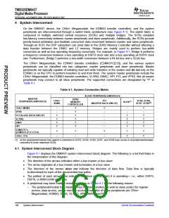
TMS320DM6437
Digital Media Processor
www.ti.com
SPRS345B–NOVEMBER 2006–REVISED MARCH 2007
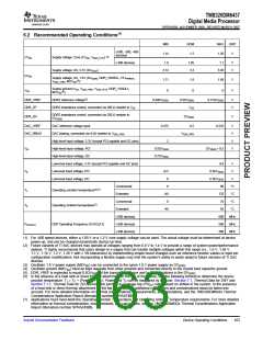
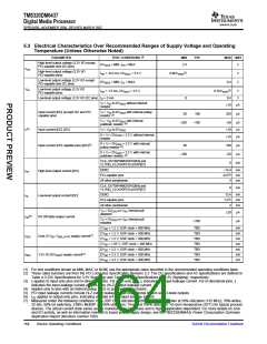
5.3 Electrical Characteristics Over Recommended Ranges of Supply Voltage and Operating
Temperature (Unless Otherwise Noted)
(1)
PARAMETER
TEST CONDITIONS
MIN
TYP
MAX UNIT
High-level output voltage (3.3V I/O except
PCI-capable and I2C pins)
DVDD33 = MIN, IOH = MAX
2.4
V
VOH
High-level output voltage (3.3V I/O
PCI-capable pins)
(2)
IOH = -0.5 mA, DVDD33 = 3.3 V
DVDD33 = MIN, IOL = MAX
0.9DVDD33
V
Low-level output voltage (3.3V I/O except
PCI-capable and I2C pins)
0.4
V
VOL
Low-level output voltage (3.3V I/O
PCI-capable pins)
(2)
IOH = 1.5 mA, DVDD33 = 3.3 V
0.1DVDD33
V
V
Low-level output voltage (3.3V I/O I2C pins) IO = 3 mA
VI = VSS to DVDD33 without internal
0
0.4
±10
µA
resistor
Input current [DC] (except I2C and PCI
capable pins)
VI = VSS to DVDD33 with internal pullup
resistor
50
100
250
µA
(4)
VI = VSS to DVDD33 with internal
pulldown resistor
–250
–100
–50
±10
±10
µA
µA
µA
(4)
II(3)
Input current [DC] (I2C)
VI = VSS to DVDD33
0 < VI < DVDD33 = 3.3 V without internal
resistor
0 < VI < DVDD33 = 3.3 V with internal
pullup resistor
Input current (PCI capable pins) [DC](5)
50
190
–50
8
µA
µA
(4)
0 < VI < DVDD33 = 3.3 V with internal
–190
(4)
pulldown resistor
CLK_OUT0/PWM2/GPIO[84] and
VLYNQ_CLOCK/PCICLK/GP[57]
mA
DDR2
–13.4 mA
–0.5(2) mA
IOH
High-level output current [DC]
PCI-capable pins
All other peripherals
4
8
mA
mA
CLK_OUT0/PWM2/GPIO[84] and
VLYNQ_CLOCK/PCICLK/GP[57]
DDR2
13.4 mA
1.5(2) mA
IOL
Low-level output current [DC]
I/O Off-state output current
PCI-capable pins
All other peripherals
4
mA
VO = DVDD33 or VSS; internal pull
disabled
±20
µA
(6)
IOZ
VO = DVDD33 or VSS; internal pull
enabled
±100
µA
CVDD = 1.2 V, DSP clock = 600 MHz
CVDD = 1.2 V, DSP clock = 500 MHz
CVDD = 1.2 V, DSP clock = 400 MHz
CVDD = 1.05 V, DSP clock = 400 MHz
DVDD = 3.3 V, DSP clock = 600 MHz
DVDD = 3.3 V, DSP clock = 500 MHz
DVDD = 3.3 V, DSP clock = 400 MHz
TBD
TBD
TBD
TBD
TBD
TBD
TBD
mA
mA
mA
mA
mA
mA
mA
ICDD
Core (CVDD, VDDA_1P1V) supply current(7)
IDDD
3.3V I/O (DVDD33) supply current(7)
(1) For test conditions shown as MIN, MAX, or NOM, use the appropriate value specified in the recommended operating conditions table.
(2) These rated numbers are from the PCI Local Bus Specification Revision 2.3. The DC specifications and AC specifications are defined in
Table 4-3 (DC Specifications for 3.3V Signaling) and Table 4-4 (AC Specifications for 3.3V Signaling), respectively.
(3) II applies to input-only pins and bi-directional pins. For input-only pins, II indicates the input leakage current. For bi-directional pins, II
indicates the input leakage current and off-state (Hi-Z) output leakage current.
(4) Applies only to pins with an internal pullup (IPU) or pulldown (IPD) resistor.
(5) PCI input leakage currents include Hi-Z output leakage for all bidirectional buffers with 3-state outputs.
(6) IOZ applies to output-only pins, indicating off-state (Hi-Z) output leakage current.
(7) Measured under the following conditions: 60% DSP CPU utilization; DDR2 Memory Controller at 50% utilization (135 MHz), 50% writes,
32 bits, 50% bit switching; 2-MHz McBSP at 100% utilization; Timer0 at 100% utilization. At room temperature (25°C) for typical process
devices. The actual current draw varies across manufacturing processes and is highly application-dependent. For more details on core
and I/O activity, as well as information relevant to board power supply design, see the TMS320DM643x Power Consumption Summary
Application Report (literature number TBD).
164
Device Operating Conditions
Submit Documentation Feedback

 TI [ TEXAS INSTRUMENTS ]