TMS320DM6437
Digital Media Processor
www.ti.com
SPRS345B–NOVEMBER 2006–REVISED MARCH 2007
5 Device Operating Conditions
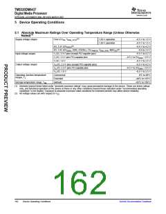
5.1 Absolute Maximum Ratings Over Operating Temperature Range (Unless Otherwise
Noted)(1)
Supply voltage ranges:
(2)
Core (CVDD, VDDA_1P1V
)
1.05-V operation
1.20-V operation
–0.5 V to 1.5 V
–0.5 V to 1.5 V
(2)
I/O, 3.3V (DVDD33
)
–0.5 V to 4.2 V
(2)
I/O, 1.8V (DVDDR2, DDR_VDDDLL, PLLPWR18, VDDA_1P8V, MXVDD
)
–0.5 to 2.5 V
Input voltage ranges:
Output voltage ranges:
VI I/O, 3.3-V pins (except PCI-capable pins)
VI I/O, 3.3-V pins PCI-capable pins
VI I/O, 1.8 V
–0.5 V to 4.2 V
–0.5 V to DVDD33 + 0.5 V
–0.5 V to 2.5 V
VO I/O, 3.3-V pins (except PCI-capable pins)
VO I/O, 3.3-V pins PCI-capable pins
VO I/O, 1.8 V
–0.5 V to 4.2 V
–0.5 V to DVDD33 + 0.5 V
–0.5 V to 2.5 V
Operating Junction temperature
ranges, TJ:
Commercial
0°C to 90°C
Extended
–40°C to 125°C
–65°C to 150°C
Storage temperature range, Tstg
(default)
(1) Stresses beyond those listed under "absolute maximum ratings" may cause permanent damage to the device. These are stress ratings
only, and functional operation of the device at these or any other conditions beyond those indicated under "recommended operating
conditions" is not implied. Exposure to absolute-maximum-rated conditions for extended periods may affect device reliability.
(2) All voltage values are with respect to VSS.
162
Device Operating Conditions
Submit Documentation Feedback

 TI [ TEXAS INSTRUMENTS ]