TMS320DM6437
Digital Media Processor
www.ti.com
SPRS345B–NOVEMBER 2006–REVISED MARCH 2007
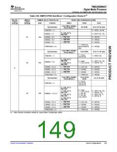
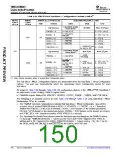
Table 3-54. EMIFA/VPSS Sub-Block 1 Configuration Choices E and G(1)
MAJOR
CONFIG
OPTION
MINOR
CONFIG
OPTION
PINMUX SELECTION FIELDS
RESULTING PERIPHERALS/PINS
VPBE
AEM
OTHERS
EMIFA
GPIO
8-bit EMIFA (NAND)
Pinout Mode 5
Cfg Summary
No VENC
14-to-18 GP pins
0 = GP[31, 29:22]
0 = GP[11:10, 7:5]
VENCSEL = 0
0 = EM_D[7:0]
-
-
0 = EM_A[2:1],
EM_CS2
RGBSEL = 0
E1,G1
101
CS3SEL = 0,1
CS4SEL = 0,1
CS5SEL = 0,1
1 = EM_CS3
1 = EM_CS4
1 = EM_CS5
-
-
-
0 = GP[13]
0 = GP[32]
0 = GP[33]
1 = VPBECLK, can
be used by DAC
VPBECKEN = 0,1
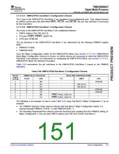
Cfg Summary
VENCSEL = 1
-
0 = GP[30]
8-bit EMIFA (NAND)
Pinout Mode 5
E,G
8-bit VENC
4-to-9 GP pins
1 = VCLK,
YOUT[7:0]
1 = EM_D[7:0]
-
0 = EM_A[2:1],
EM_CS2
1 = EM_A[2:1],
EM_CS2
0 = none
1 = LCD_FIELD
0 = GP[11:10, 7:5]
1 = GP[10, 7:5]
RGBSEL = 0,1
E2,G2
101
CS3SEL = 0,1,2
CS4SEL = 0,1,2
CS5SEL = 0,1,2
VPBECKEN = 0,1
1 = EM_CS3
1 = EM_CS4
1 = EM_CS5
-
2 = LCD_OE
2 = VSYNC
2 = HSYNC
1 = VPBECLK
0 = GP[13]
0 = GP[32]
0 = GP[33]
0 = GP[30]
(1) Italics indicate mandatory setting for a given Minor Configuration option.
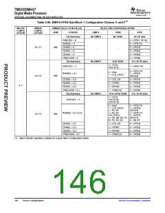
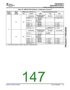
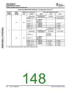
The Sub-Block 1 Minor Configuration Options are independent from the Sub-Block 0 Minor Configuration
Options. The user can independently select the appropriate Minor Configuration Option for each
Sub-Block.
As shown in Table 3-50 through Table 3-54, the configuration choices of the EMIFA/VPSS Sub-Block 1
are determined by the following PINMUX register fields:
•
PINMUX0 register fields AEM, VENCSEL, RGBSEL, CS3SEL, CS4SEL, CS5SEL, and VPBECKEN.
The following is an example on how to read Table 3-50 through Table 3-54 using Sub-Block 1 Minor
Configuration G2 as an example:
•
•
The PINMUX Selection Fields columns indicate that Sub-Block 1 Minor Configuration Option G2 is
selected through setting PINMUX0 fields to AEM = 5, VENCSEL = 1, RGBSEL = 0 or 1 (based on
whether the VPBE LCD_FIELD pin is needed), CS3SEL = 0/1/2 (based on the desired pin choice),
CS4SEL = 0/1/2 (based on the desired pin choice), CS5SEL = 0/1/2 (based on the desired pin choice),
and VPBECKEN = 0/1 (based on whether VPBE VPBECLK is needed).
The Resulting Peripherals/Pins columns show the functional pins resulting from the PINMUX setting.
For example, PINMUX0.VENCSEL = 1 gives you the VCLK and YOUT[7:0] pins for the VPBE, in
addition to EM_D[7:0] pins for the EMIFA. PINMUX0.RGBSEL = 1 gives you the LCD_FIELD pin for
the VPBE, along with EM_A[2:1] and EM_CS2 for the EMIFA, and 4 GP pins.
150
Device Configurations
Submit Documentation Feedback

 TI [ TEXAS INSTRUMENTS ]