TMS320DM6437
Digital Media Processor
www.ti.com
SPRS345B–NOVEMBER 2006–REVISED MARCH 2007
3.7.3.13.7 EMIFA/VPSS Block Pin-By-Pin Multiplexing Summary
This section summarizes the EMIFA/VPSS Block muxing on a pin-by-pin basis. It provides an alternative
view to pin muxing in the EMIFA/VPSS Block. This section should only be used after following the
procedures listed in Section 3.7.3.13.1 to determine the actual EMIFA/VPSS Configuration Option for the
application need.
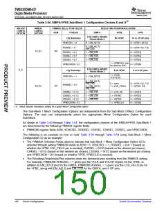
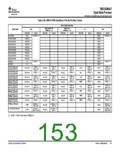
Table 3-56 shows the pin multiplexing control for each pin in the EMIFA/VPSS Sub-Block 0. These are the
fields in the PINMUX0 and PINMUX1 registers that control the multiplexing in this sub-block:
•
PINMUX0: AEM, AEAW, CWENSEL, CFLDSEL, CI10SEL, CI32SEL, CI54SEL, CI76SEL, CCDCSEL,
HVDSEL
•
PINMUX1: PCIEN
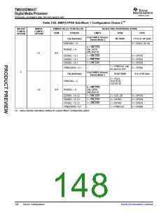
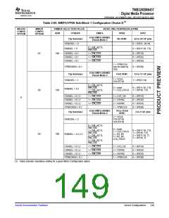
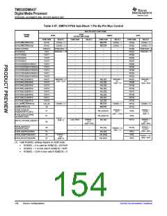
Table 3-57 shows the pin multiplexing control for each pin in the EMIFA/VPSS Sub-Block 1. These are the
fields in the PINMUX0 register that control the multiplexing in this sub-block:
•
PINMUX0: AEM, VENCSEL, RGBSEL, CS5SEL, CS4SEL, CS3SEL, VPBECKEN
EMIFA/VPSS Sub-Block 2 is dedicated to EMIFA pins EM_WAIT/(RDY/BSY), EM_OE, and EM_WE.
There is no pin multiplexing in this block. These pins always function as EMIFA control pins.
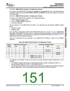
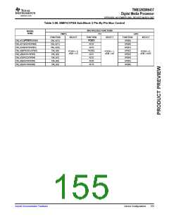
Table 3-58 shows the pin multiplexing control for each pin in the EMIFA/VPSS Sub-Block 3. These are the
fields in the PINMUX0 and PINMUX1 registers that control the multiplexing in this sub-block:
•
•
PINMUX0: AEM
PINMUX1: PCIEN
152
Device Configurations
Submit Documentation Feedback

 TI [ TEXAS INSTRUMENTS ]