TMS320DM6437
Digital Media Processor
www.ti.com
SPRS345B–NOVEMBER 2006–REVISED MARCH 2007
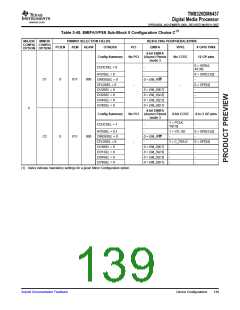
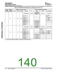
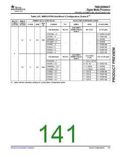
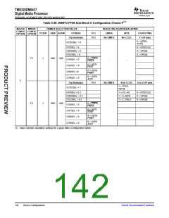
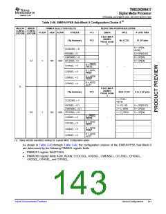
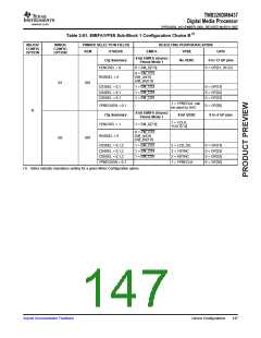
Table 3-49. EMIFA/VPSS Sub-Block 0 Configuration Choice G(1)
MAJOR
CONFIG CONFIG
OPTION OPTION
MINOR
PINMUX SELECTION FIELDS
AEM AEAW OTHERS
RESULTING PERIPHERALS/PINS
PCIEN
PCI
PCI
EMIFA
VPFE
# GPIO PINS
13 GP pins
8-bit EMIFA
(NAND)
Pinout mode
5
Cfg Summary
No CCDC
0 = GP[54,
43:36]
CCDCSEL = 0
-
HVDSEL = 0
-
-
-
0 = GP[53:52]
0 = GP[35]
0 = GP[34]
CWENSEL = 0
G1
1
101
000 CFLDSEL = 0
0 = PREQ,
PINTA
CI10SEL = 0
-
-
-
-
-
-
0 = AD31,
PRST
CI32SEL = 0
CI54SEL = 0
CI76SEL = 0
0 = AD29,
PGNT
0 = AD25,
AD27
G
8-bit EMIFA
(NAND)
Pinout mode
5
Cfg Summary
PCI
8-bit CCDC
0-to-4 GP pins
1 = PCLK,
YI[7:0]
CCDCSEL = 1
-
-
HVDSEL = 0,1
CWENSEL = 0,1
-
-
-
1 = VD, HD
1 = C_WEN
1 = C_FIELD
0 = GP[53:52]
0 = GP[35]
0 = GP[34]
G2
1
101
000 CFLDSEL = 0,1
0 =PREQ,
PINTA
CI10SEL = 0
CI31SEL = 0
CI54SEL = 0
CI76SEL = 0
-
-
-
-
-
-
-
-
-
0 = AD31,
PRST
0 = AD29,
PGNT
0 = AD25,
AD27
(1) Italics indicate mandatory settings for a given Minor Configuration option.
As shown in Table 3-43 through Table 3-49, the configuration choices of the EMIFA/VPSS Sub-Block 0
are determined by the following PINMUX register fields:
•
•
PINMUX1 register field PCIEN
PINMUX0 register fields AEM, AEAW, CCDCSEL, HVDSEL, CWENSEL, CFLDSEL, CI10SEL,
CI32SEL, CI54SEL, and CI76SEL.
Submit Documentation Feedback
Device Configurations
143

 TI [ TEXAS INSTRUMENTS ]