TMS320DM6437
Digital Media Processor
www.ti.com
SPRS345B–NOVEMBER 2006–REVISED MARCH 2007
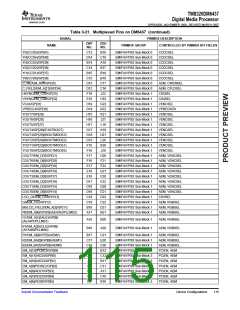
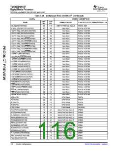
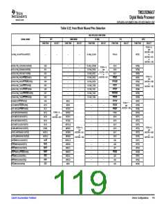
Table 3-21. Multiplexed Pins on DM6437 (continued)
SIGNAL
PINMUX DESCRIPTION
ZWT
NO.
ZDU
NO.
NAME
PINMUX GROUP
CONTROLLED BY PINMUX BIT FIELDS
HECC_RX/TINP1L/URXD1/GP[56]
HECC_TX/TOUT1L/UTXD1/GP[55]
CLKS1/TINP0L/GP[98]
CLKS0/TOUT0L/GP[97]
URXD0/GP[85]
L4
K4
K2
J4
P3
N3
L2
Timer 1 Block
Timer 1 Block
TIM1BK
TIM1BK
TIM0BK
TIM0BK
UR0DBK
UR0DBK
UR0FCBK
UR0FCBK
CKOBK
Timer 0 Block
L3
Timer 0 Block
L2
K3
L1
L3
M1
M2
N1
P1
M3
R1
UART0 Data Block
UART0 Data Block
UART0 Flow Control Block
UART0 Flow Control Block
CLKOUT Block
UTXD0/GP[86]
UCTS0/GP[87]
URTS0/PWM0/GP[88]
CLKOUT0/PWM2/GP[84]
Note: PINMUX groups EMIFA/VPSS Sub-Block 2 and PCI Data Block are not shown in the above table
because there is no actual pin multiplexing in those blocks. But these two blocks are still considered "pin
mux blocks" because they contain some of the pins necessary for EMIFA and PCI, respectively. The pins
in these blocks are as follows:
•
EMIFA/VPSS Sub-Block 2
–
–
–
EM_WAIT/(RDY/BSY)
EM_OE
EM_WE
•
PCI Data Block
–
–
–
AD30
AD28
AD26
Submit Documentation Feedback
Device Configurations
117

 TI [ TEXAS INSTRUMENTS ]