TMS320DM6437
Digital Media Processor
www.ti.com
SPRS345B–NOVEMBER 2006–REVISED MARCH 2007
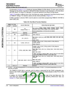
3.7.3.4 PCI Data Block
This block of 3 pins consists of 3 PCI Address/Data pins—AD30, AD28, AD26. The PINMUX1.PCIEN
register field affects the pin functions in the PCI Data Block.
As discussed in Section 3.7.3.2, Peripherals Spanning Multiple Pin Mux Blocks, PCI pins span across the
following Pin Mux Blocks: Host Block, EMIFA/VPSS Block Sub-Block 0 and Sub-Block 3, PCI Data Block,
and GPIO Block. For proper PCI operation, PCI must be selected in all of these Pin Mux Blocks.
The 3 pins in the PCI Data Block are not muxed with any other peripherals. However, the
PINMUX1.PCIEN field controls the internal pullup/pulldown resistors on these pins. For PCI operation
(PCIEN = 1), the internal pullup/pulldown resistors are disabled. If the device does not support PCI
(PCIEN = 0), the internal pullup/pulldown resistors on these pins are enabled so that the user can leave
these pins unconnected on the board.
Table 3-24 shows the Host Block pin selection based on PINMUX1.PCIEN setting.
Table 3-24. PCI Data Block Pin Control
PINMUX1.PCIEN
BLOCK FUNCTION
RESULTING PIN FUNCTIONS
No Connect Pins
(Default if PCIEN = 0)
No Connect Pins
0
Internal pullup/pulldown enabled. Leave these three pins unconnected on the board.
PCI
1
PCI: AD26, AD28, AD30
(Default if PCIEN = 1)
Submit Documentation Feedback
Device Configurations
121

 TI [ TEXAS INSTRUMENTS ]